
In this blog entry, I will introduce the printed circuit board (PCB) design flow. I will then proceed to focus on the schematic capture section of the PCB design flow by using the KiCad PCB design tool to create a schematic for a simple LED blinker circuit. The PCB layout section of the design flow is covered in this blog entry.
PCB Design Flow
The PCB design flow is illustrated in Figure 1. It can be broken into two major steps:
- Schematic Creation: This is where the circuit schematic will be ‘captured’ by the PCB design tool.
- Layout Creation: This is where the circuit schematic will be turned into a PCB layout containing matching footprints for the various components in the circuit, and traces representing the wires/nets connecting these components.
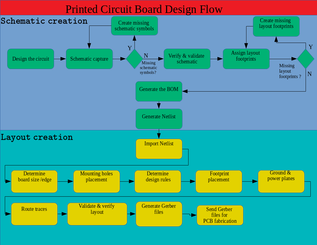
Each one of these steps can be broken down into further smaller steps.
Schematic Creation Overview
A circuit schematic is an illustrative diagram demonstrating how a variety of electrical/electronic components represented by schematic symbols, are wired together.
Here the designer inputs the schematic into KiCad’s schematic capture (editor) tool. If one or more components in the circuit is not available in the schematic symbols library, the designer must create a new schematic symbol and add it to the schematic. The procedure for schematic symbol creation is beyond the scope of this tutorial. It may be covered in a future blog entry.
Once the schematic is completed and verified, a footprint assignment tool is then used to assign every schematic symbol in the schematic to a layout footprint. If one or more components (schematic symbols) in the design have no valid footprint(s) in the footprint library, the designer must create a suitable footprint, before mapping it to its appropriate schematic symbol. The procedure for layout footprint creation is yet again outside the scope of this tutorial and may be covered in a future blog entry.
At this point, the user can generate the bill of materials (BOM) list containing a list of all the components required by the schematic, and generate the schematic netlist. The schematic netlist is simply a file that textually describes all the components and the interconnections / wiring between them as illustrated in the schematic.
Layout Creation Overview
Here the designer will first open KiCad’s PCB / layout editor tool, and set the appropriate design rules for the layout. The design rules are determined by the PCB manufacturer and ensure that the KiCad layout design meets the specifications required for successful fabrication.
The designer will then import the schematic netlist into the layout editor tool and create the PCB’s outline via the ‘Edge.Cuts’ (board edge) layer. Copper fills / pours for ground planes and other zones are then allocated within the PCB outline.
Next, all component footprints are placed within the PCB outline and the traces between the components are routed (as per the wires/nets in the schematic). Once the layout is complete, the designer will perform a design rule check (DRC) to ensure that the layout meets all the design rules and can indeed be fabricated by the PCB manufacturing house. The final step is to generate the layout’s Gerber files and send them to the PCB manufacturing house for fabrication.
Schematic Symbol vs Layout Footprint
Schematic symbols denote the schematic representation of a component. For example, the schematic symbol of a resistor is shown in Figure 2. Note that because a schematic symbol is an abstract illustration representing a component, it’s exact size, placement and dimensions matters in so far as to ensure that the schematic is clear, uncluttered and legible. The size & position of the schematic symbol does not translate into the physical world.

Layout footprints on the other hand are just that, the footprint representation that will be ‘printed on & drilled into’ the printed circuit board. Layout footprints typically consists of a silkscreen portion outlining the size and shape of the component to be placed, and copper through hole / surface mount pads that connect the components pins to the traces on the PCB.
The dimensions of the layout footprint must match the dimensions of the component that it represents. Since the component will be placed onto its layout footprint in the physical world. The placement of the footprint must also be well thought out. Figure 3 illustrates a matching layout footprint for the resistor schematic symbol in Figure 2.

Introduction to KiCad
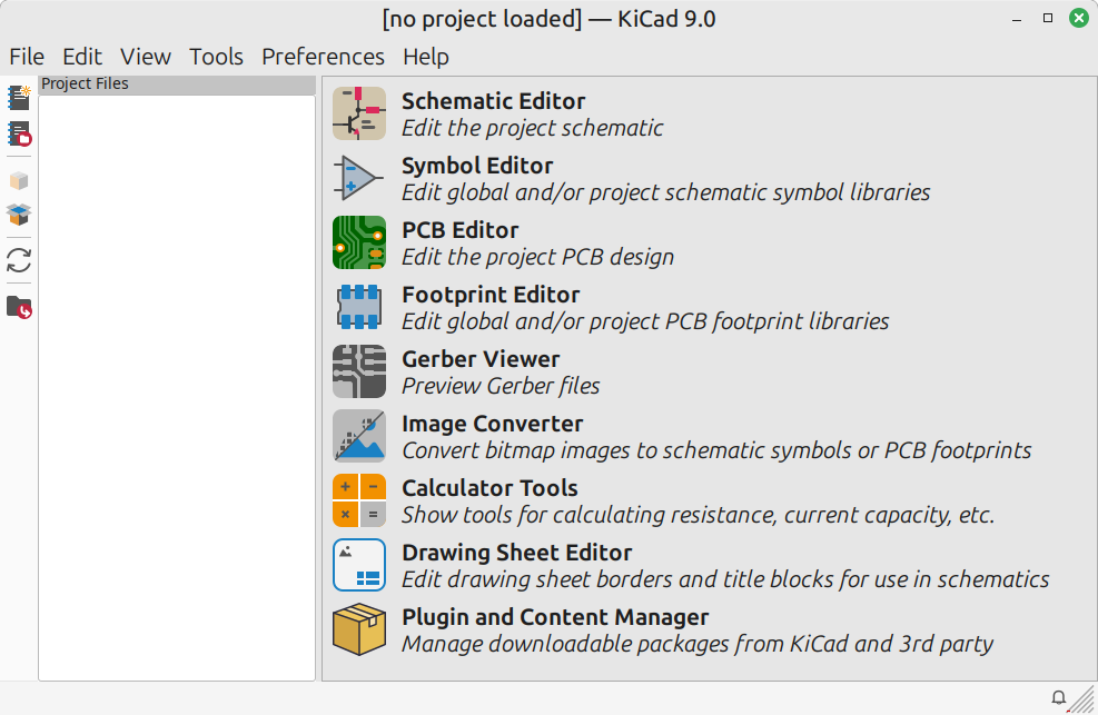
When the KiCad application runs, the first thing the user sees is the main KiCad window, From this window, a variety of tools can be accessed including:
- Schematic editor – used for schematic capture
- Symbol (Schematic) editor – used to edit existing schematic symbols and create new ones
- PCB layout editor – used for PCB layout design
- Footprint editor – used to edit existing layout footprints and create new ones
- Gerber viewer – used to inspect Gerber files
- Image Converter – used for creating logos from bitmap images among other things
- Calculator tools – used for various calculations i.e. calculate current capacity of a trace
- Drawing sheet editor – edit drawing sheet borders and title blocks for use in schematics and PCB designs
- Plugin and content Manager – Manage downloadable packages from KiCad and 3rd party repositories.
Creating a New Project
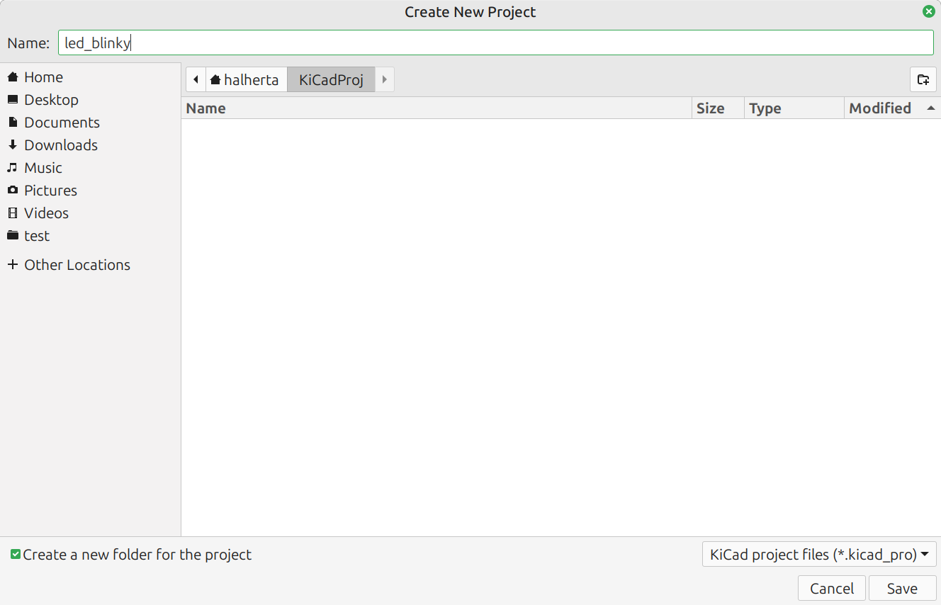
Create a new root directory where all KiCad projects will be saved. Call this directory KiCadProj or some other relevant name,
In KiCad goto File->New Project
Create a new project called led_blinky and save it in the KiCadProj directory. This will automatically create a folder name led_blinky under the KiCadProj directory and create a .kicad_pro project file in it. All other files related to this project i.e. schematic, layout, netlist e.t.c. will be saved into this folder.
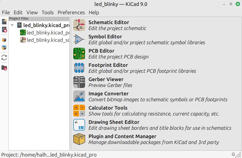
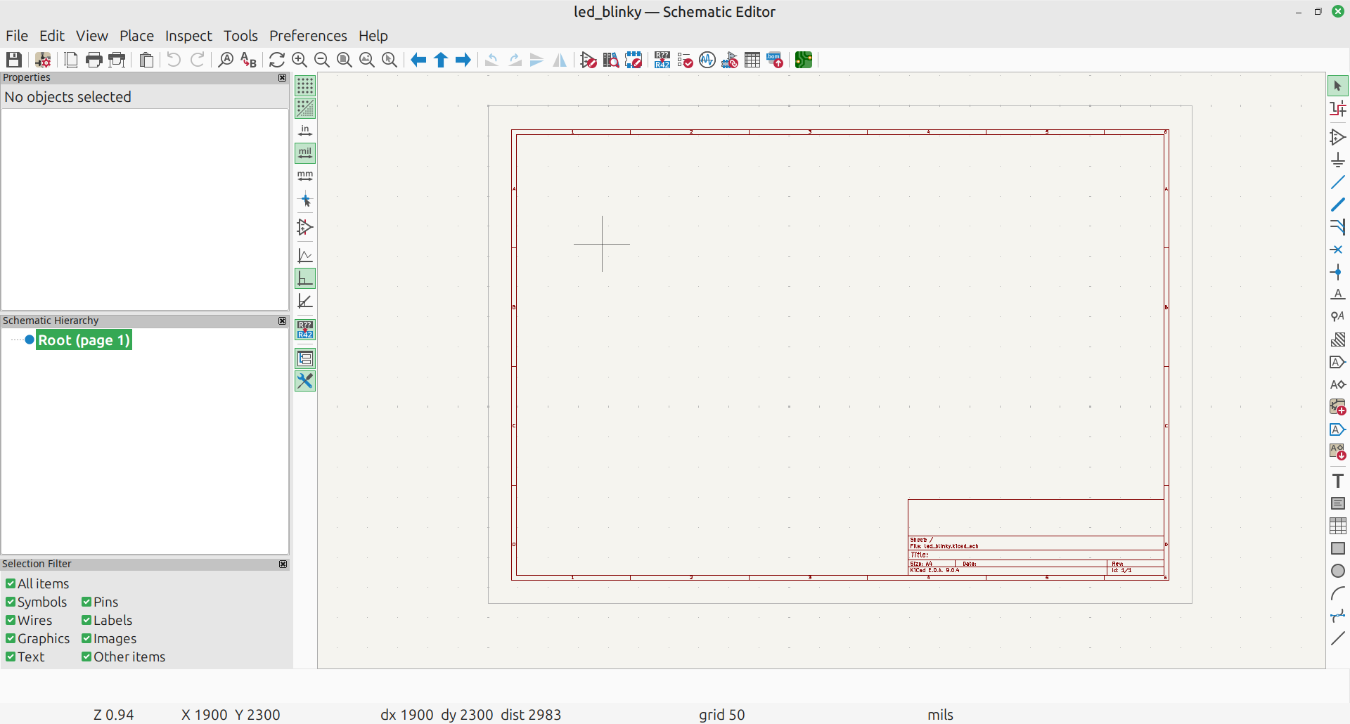
As per the PCB Design flow shown in Figure 1, start with the schematic creation process. To do this select the Schematic Editor from the main KiCad Window. This will open the schematic editor application window shown in Figure 7.
The Astable Multivibrator Circuit
The transistor based astable multivibrator circuit shown in the schematic below is a simple square wave oscillator. It generates two square waves that exhibit a 180 degree phase shift. For more on the theory behind this circuit’s operation, the curious reader can go here.
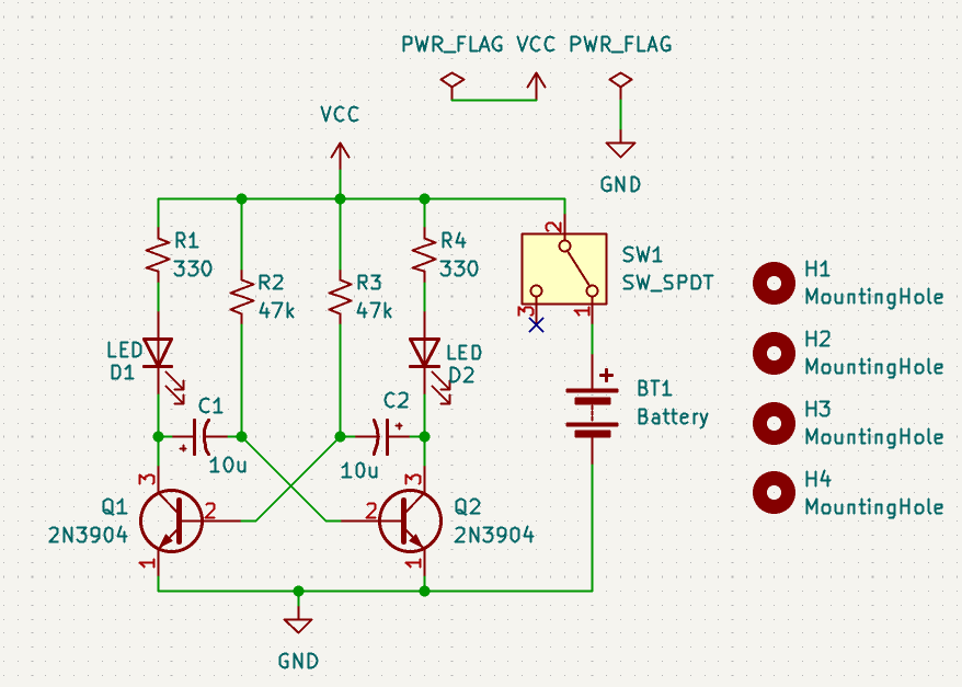
Connecting LED’s to the collector of each transistor turns the circuit into an LED flasher. The frequency of oscillation is a function of the values of R2, R3, C1 & C2 and is approximately equal to :
$$f = \frac{1}{ln(2) \times (R_2C_1 + R_3C_2)}$$
Assuming that \(R_2 = R_3 = R \) and \(C_1 = C_2 = C \), the frequency of oscillation becomes,
$$f = \frac{1}{ln(2) \times RC }$$
KiCad Schematic Editor
KiCad’s schematic editor is quite powerful and integrates a ton of functionality. Some of which will be covered in this section.
Hotkeys
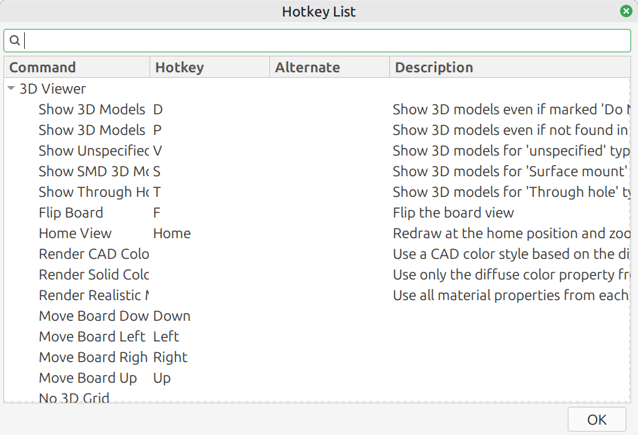
Let’s start with the schematic editor from the KiCad main window. Before going any further, it is important to familiarize yourself with the hotkeys available within KiCad. It might not seem necessary, but it is well worth your time to memorize the hotkeys for some of the more commonly used actions. To get the list, go to Help->List Hotkeys or press Ctrl-F1 and look under the Schematic Editor listview. Things that can be done easily with hotkeys in the schematic editor are listed below:
- e – Edit properties of a component
- m – Move a component
- ctrl+D – Duplicate (Copy) a component
- r – Rotate a component
- x – Mirror a component along the X axis
- y – Mirror a component along the Y axis
- a – Add a component
- t – Add Schematic text
- Delete – Delete a component
Using these shortcuts/hotkeys will make working with KiCad much faster and efficient.
Page Settings
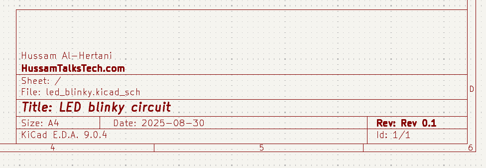
To fill in the legend in the bottom left hand corner, go to File->Page Settings , and fill in the various details i.e. revision number, date, title e.t.c. The page size and orientation can also be changed from the Page Settings dialog.
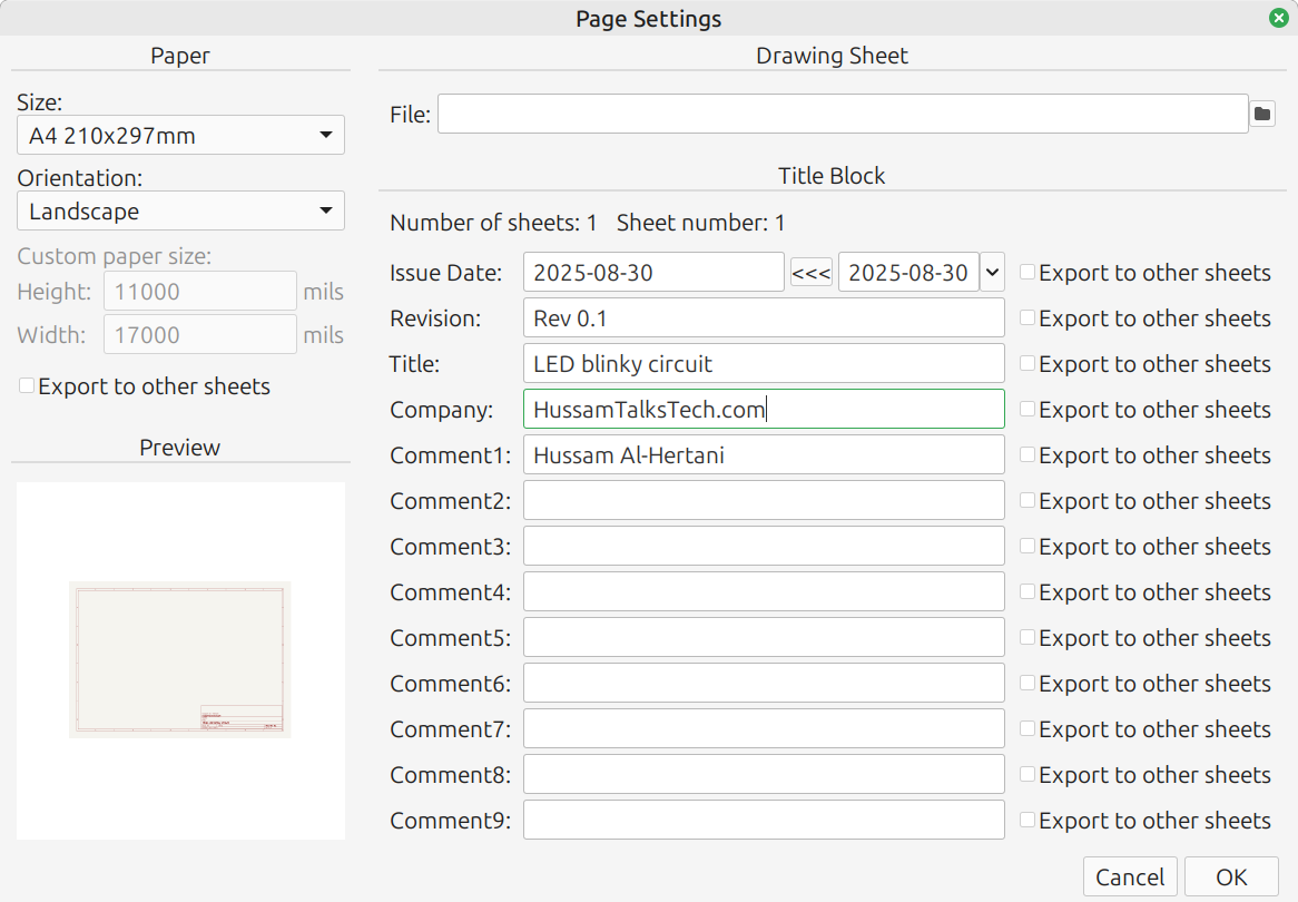
Once you are done with the page settings,the legend will be updated as shown in Figure 10.
Zooming in & out
To quickly zoom in and out of the schematic area one can use the mouse scroll wheel. Alternatively, you can also use the zoom icons in the center of the top toolbar.
Schematic capture
Now we add the components to the schematic! To add components, use the shortcut ‘a’ or click on the op-amp icon (triangular three pin component with a ‘+’ and ‘-’ signs on its inputs) in the top righthand corner; to open the Choose Symbol dialog shown in Figure 12.
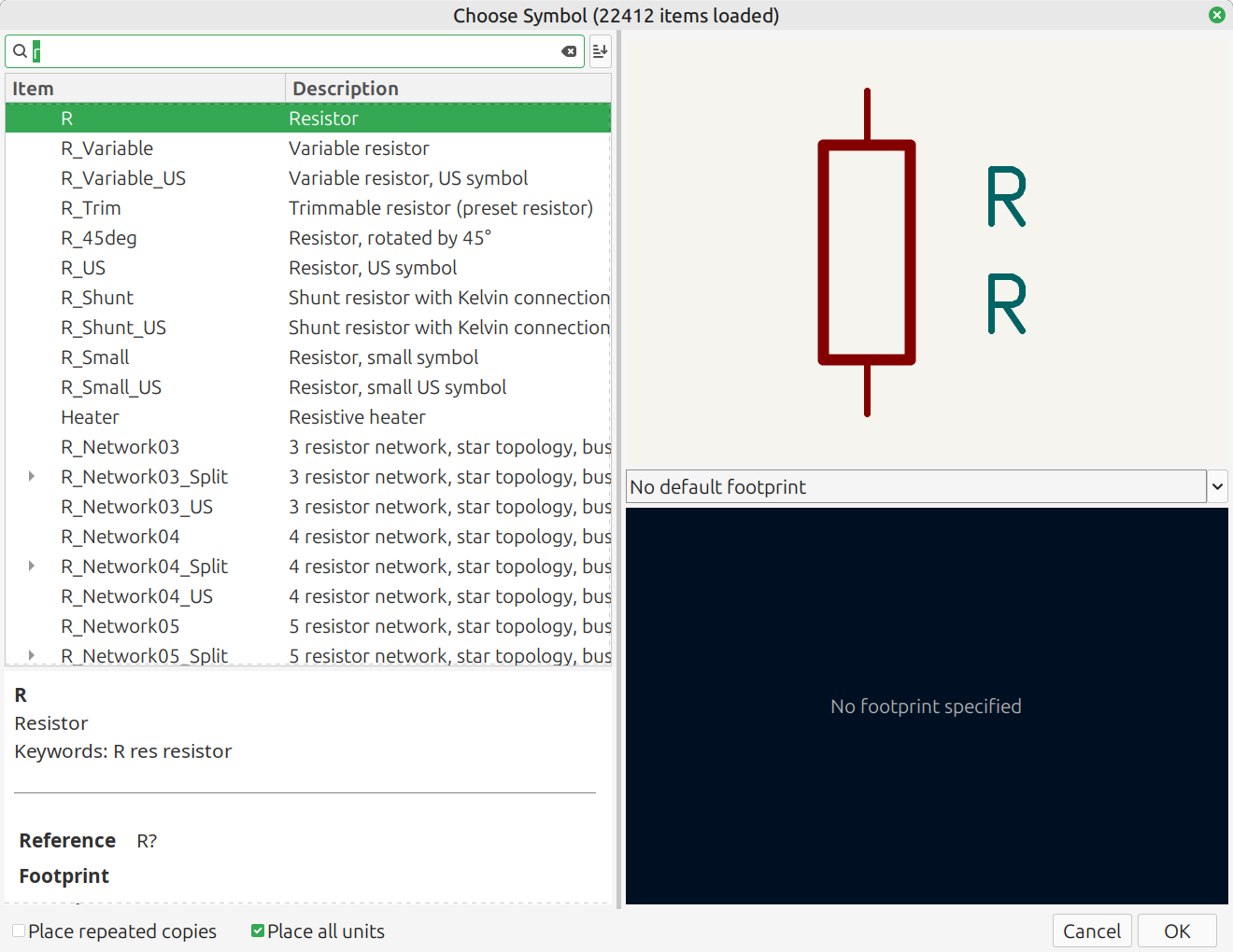
The following schematic symbols will be needed. You should be able to search for them inside the Choose Symbol dialog:
- Two NPN transistors.2N3904 should be fine.
- Four Resistors. Select component R_Small_US. R, R_US and R_Small can also be used.
- Two Capacitors. Select component C_Polarized_Small_US. Any capacitor symbol with polarity will work, since this circuit utilizes polarized electrolytic capacitors.
- Two Light emitting diodes (LED)s. Select component LED. LED_Small can also be used.
- A power symbol. Select component Battery.
- A ground symbol. Select component GND.
- Four mounting holes. Select component MountingHole.
- An SPDT (single pole double throw) switch SW_SPDT.
Once these components are added to the schematic, use hotkeys to copy (c), move(m), delete(Delete), edit part values(e), rotate (r) and/or mirror(x/y) these components as needed. You can also right click on the component and a context menu will pop up giving you similar functionality. The hotkeys will make things go faster however.
Once all the parts are placed, connect them with wires. To start a wire you can use the hotkey (w) or click on the diagonal thin blue wire icon (Add a Wire) on the right toolbar. By default all wires are straight. To draw the diagonal wires, you’ll have to click on the Line modes for wires and buses (45 deg) icons. They are located on the left toolbar and has a small picture of two lines cutting each other at a 90 degree angle, with a third line at a 45 degree angle. Alternatively, you can use the Shift+Space shortcut.
Additionally, make sure you add a no connect flag to pin 3 of the SPDT switch (as shown in Figure 7). This can be accomplished with the hotkey Q or by selecting the ‘x’ icon in the right toolbar.
Once completed, the schematic should look almost similar the one in Figure 7 (less the power flags, which will be discussed in the next section). Make sure that all components are assigned the correct values.
Component Annotation and the Electrical Rule Check (ERC)
Notice that each symbol come with two textual descriptions;
- a reference such as R1, R2, C1, Q1, D2, SW1, BT1 e.t.c, and a
- name such as SW-SPDT or LED. Notice that for passive components, the name field ends up being set to their component values i.e. 330, 10u e.t.c.
Both fields can be modified by selecting the symbol in question and then either right click->Properties or pressing the ‘E’ hotkey. It is important that each symbol in the schematic has a valid and unique reference value. This is because each symbol is represented in the netlist via its reference value. For example you cannot have two resistors with the same reference number R1.
The process of giving each component a unique reference value is known as Component Annotation. The KiCad schematic editor performs annotation for us automatically so you should not have to worry about it. Note that the reference value for each symbol consists of:
- a reference designator (R for resistors, C for capacitors e.t.c.), and a
- unique number.
Different symbols get different reference designators. A list of reference designators is provided below:
- Resistor – R
- Capacitor – C
- Inductor – L
- Diode – D
- Transistor – Q
- Integrated circuit (I.C.) – U
- Connector – J
- Switch – SW
- Battery – BT
- Mounting Hole – H
Add the PWR_FLAG symbol to both the VCC (power) and GND components/symbols. The reason for this will be explained shortly. The schematic should now look identical to that shown in Figure 7.
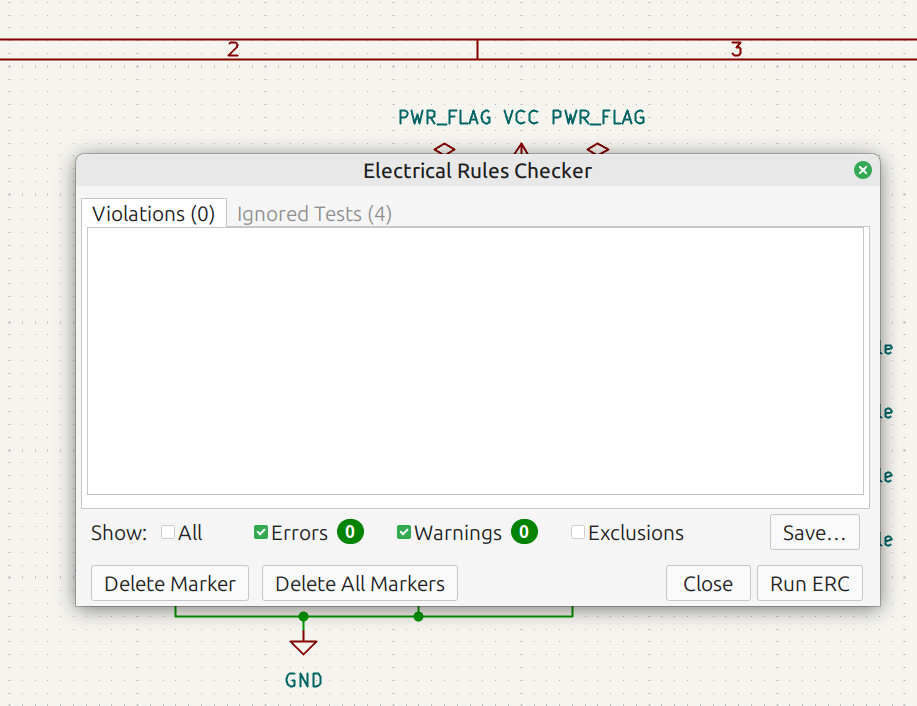
The KiCad schematic editor has a built-in Electrical Rule Check (ERC). The ERC ensures that the schematic is electrically sound and that power nets (wires) are connected to an appropriate single power driver. It also highlights floating pins e.t.c.
In order to run & pass the ERC, the current circuit needs to have a single power driver net. In our schematic, that would be the VCC net. To facilitate this, attach a PWR_FLAG symbol to both the VCC (power source) and GND (power sink) symbols. Then proceed to running the ERC check by clicking on the Perform Electrical Rules Check (checklist) icon in the top toolbar as shown in the figure below. If everything is OK, the ERC should pass successfully with no violations.
Assign Footprints to Schematic Symbols
So far the schematic has been captured and an ERC was successfully passed. The next step is to assign a layout footprint to each schematic symbol. This is necessary to prepare our design for layout. Click on the Assign Footprints icon (containing a schematic symbol of an operation amplifier and an integrated circuit footprint linked) on the top toolbar. This should open the Assign footprints dialog shown in Figure 14.
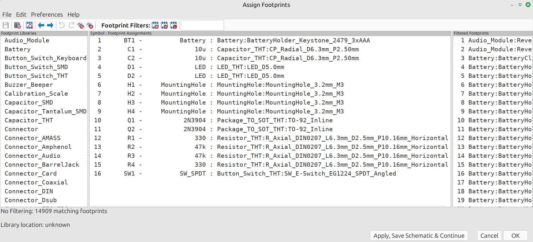
In the Assign Footprints dialog, the designer needs to assign the layout footprints in the rightmost column to the schematic symbols (with reference values) in centre column. Notice that the leftmost column has a list of the KiCad’s builtin layout footprint libraries.
The goal here is to match our schematic symbols (centre column) with appropriate layout footprints in the rightmost column. To help us achieve this goal, several filter icons are available that facilitate filtering through all the available footprints by keyword, pin count, library or search pattern.
For example, assume that the design needs a AAA battery connector with two pins (power and ground), to do this one can:
- turn on the filter footprint by library and select the ‘Battery’ library from the leftmost column,
- turn on the filter footprint by pin count, which will automatically look for all footprints with a pin count of two (same as that of the BT1 schematic symbol)
- turn on the filter footprint by search keyword or pattern and type in the adjacent text box AAA, which helps homing in on all footprints with ‘AAA’ in their names.
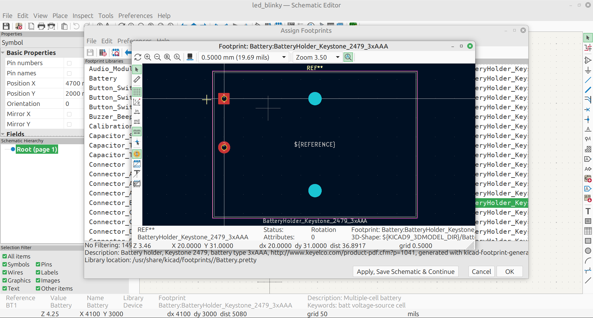
This should leave us with three options. Select the Battery:BatteryHolder_Keystone_2479_3xAAA footprint by clicking on it. Notice how its assigned to the BT1 schematic symbol in the centre column in Figure 14.
The actual footprint can be inspected by clicking on the View the selected footprint in the footprint viewer icon (IC with magnifying glass). Many of the footprints built into KiCad have part-names and/or additional dimensions information embedded in their KiCad footprint names, making it easier to search for those parts on Electronic part distributor websites like Digikey or Mouser.
In a similar manner, associate the remaining schematic symbols to the following footprints:
- BT1 – Battery:BatteryHolder_Keystone_2479_3xAAA
- C1,C2 – Capacitor_THT:CP_Radial_D6.3mm_P2.50mm
- D1,D2 – LED_THT:LED_D5.0mm
- H1-H4 – MountingHole:MountingHole_3.2mm_M3
- Q1,Q2 – 2N3904:Package_TO_SOT_THT:TO-92_Inline
- R1-R4 – Resistor_THT:R_Axial_DIN0207_L6.3mm_D2.5mm_P10.16mm_Horizontal
- SW1 – Button_Switch_THT:SW_E-Switch_EG1224_SPDT_Angled
Now click on the Apply, Save Schematic & Continue button, then the OK button.
Congratulations! You have completed the schematic capture process and are now ready to layout the board. This will be covered in a future blog entry.
1 thought on “PCB Layout Design with KiCad Part I: Introduction & Schematic Capture”