In this blog entry, the PCB layout for the astable multivibrator circuit schematic design covered in part I, will be created using the Kicad PCB Editor application. Before proceeding however the user must be made aware of the two most common measurement units and how to convert between them.
Importance of spatial dimensions and units of measurements for PCB design
Schematic capture is an abstract procedure and there’s no real need to keep in mind the dimensions of component symbols, wires nor the spacing between them. A schematic simply needs to be clean, readable and presentable.
When laying out a PCB however, the designer must be aware of the dimensions of the footprints, traces e.t.c for many reasons. For starters, a PCB layout has finite space defined by the PCB’s outline (board edge). This space must be sufficient to carry all the layout footprints and traces. The traces; which act like wires, need to be sized adequately to allow enough current to flow through them. For example, a trace with a width of 12 mils can handle about 1A of current (assuming 1 \(\frac{oz}{ft^2}\) copper depth/height). If a trace needs to handle more current, then its trace width will have to be increased.
Finally PCB manufacturing houses have things called design rules that they make available to their customers. These design rules usually include the minimum acceptable clearances required in a layout design. These tolerances exist because the equipment that fabricates PCB’s is only able to manufacture PCBs within prescribed dimensional tolerances. For example, a PCB manufacturing house can state as part of their design rules that the smallest distance/clearance between two copper traces must be 6mil. If the designer places two traces with a 4mil spacing between them, the PCB manufacturer will not be able to fabricate the board.
The two units of measurements used to measure the dimensions of footprints, traces, clearances e.t.c are millimetres (mm) and mils. 1 mil is equivalent to a thousandths of an inch and is sometimes referred to as 1 thou. In the past, the imperial unit mils used to be more popular in the PCB design and electronics world. This is why through-hole dual inline packages (DIP), a technology developed in the 70’s, has a pitch (spacing between the pins) of 100 mils or 0.1”. This is also the spacing used between tie-points on a breadboard. And while the metric mm has become more dominant, the imperial mil is still in use. As such, it is important to be able to convert between mils and mm.
To convert from mil to mm:
$$ Val_{mm} = \frac{Val_{mil} \times 25.4}{1000} $$
To convert from mm to mil:
$$ Val_{mil} = \frac{Val_{mm} \times 1000}{25.4} $$
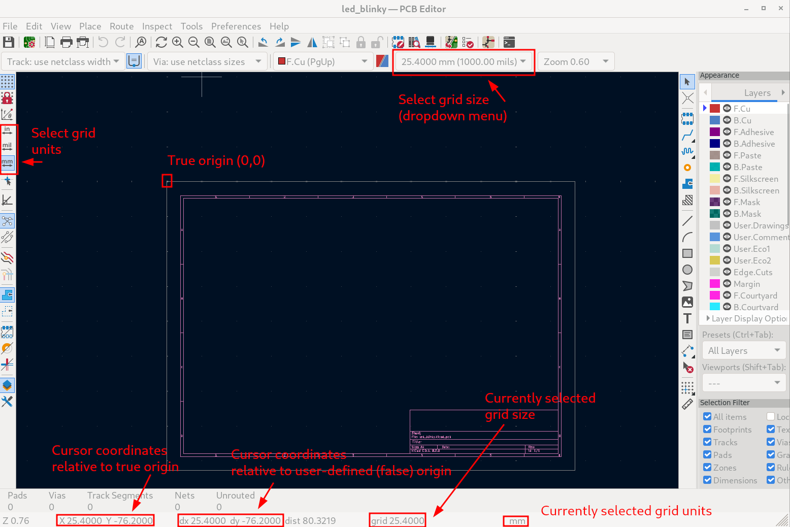
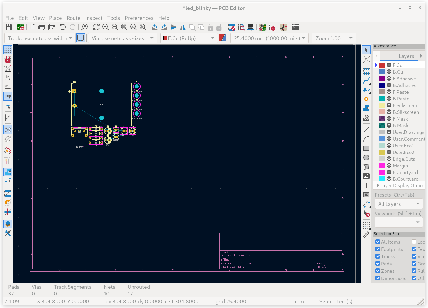
When placing moving components/traces, one must also be aware of the spacing being used by the KiCad PCB editor. The grid size can be changed via the dropdown menu shown in Figure 1. The grid units can also be changed via the icons in the left toolbar. In the grid size dropdown menu, you’ll notice that the first 12 entries are in mils (whole numbers) whereas the last 10 entries measurements are in mm (whole numbers).
The designer will want to alternate between finer and coarser grid settings during the layout process. When placing large components or drawing the PCB outline, use coarse grid setting like 10-50mil or 2.5-5mm. When placing smaller parts or laying out traces, the designer will want to switch to finer settings like 1-5 mils or 0.1-0.5mm. Custom grid sizes may also be set if needed.
The cursor coordinates can be determined by looking at the bottom status bar. The X/Y coordinates are defined with respect to the top left corner of the white outline defining the work area. The second set of coordinates; dx/dy, are defined with respect to a user-defined/false origin. This false origin can be set anywhere in the work area simply by moving the cursor there and pressing space bar. The false origin will come in very handy when sizing the PCB outline.
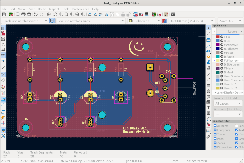
Import Netlist.
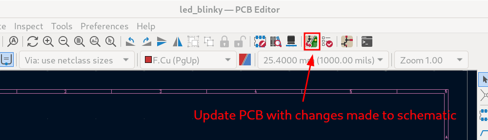
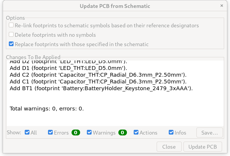
The next step is to import the netlist (design) created in the schematic editor into the layout editor. This is accomplished by pressing F8 or the icon shown in Figure 2 in the top toolbar. The Update PCB from Schematic dialog pops up as shown in Figure 3. Press the Update PCB button to see all the parts and the ratsnest connecting them.
Move the cursor to the top left corner of the layout editor’s work area and leave them there for now.
Board Setup and Establishing the Design Rules
Before proceeding with the layout, let’s have a look at the board setup. The Board Setup dialog can be accessed through the File Menu or green icon with red gear wheel in the top left corner (top toolbar).
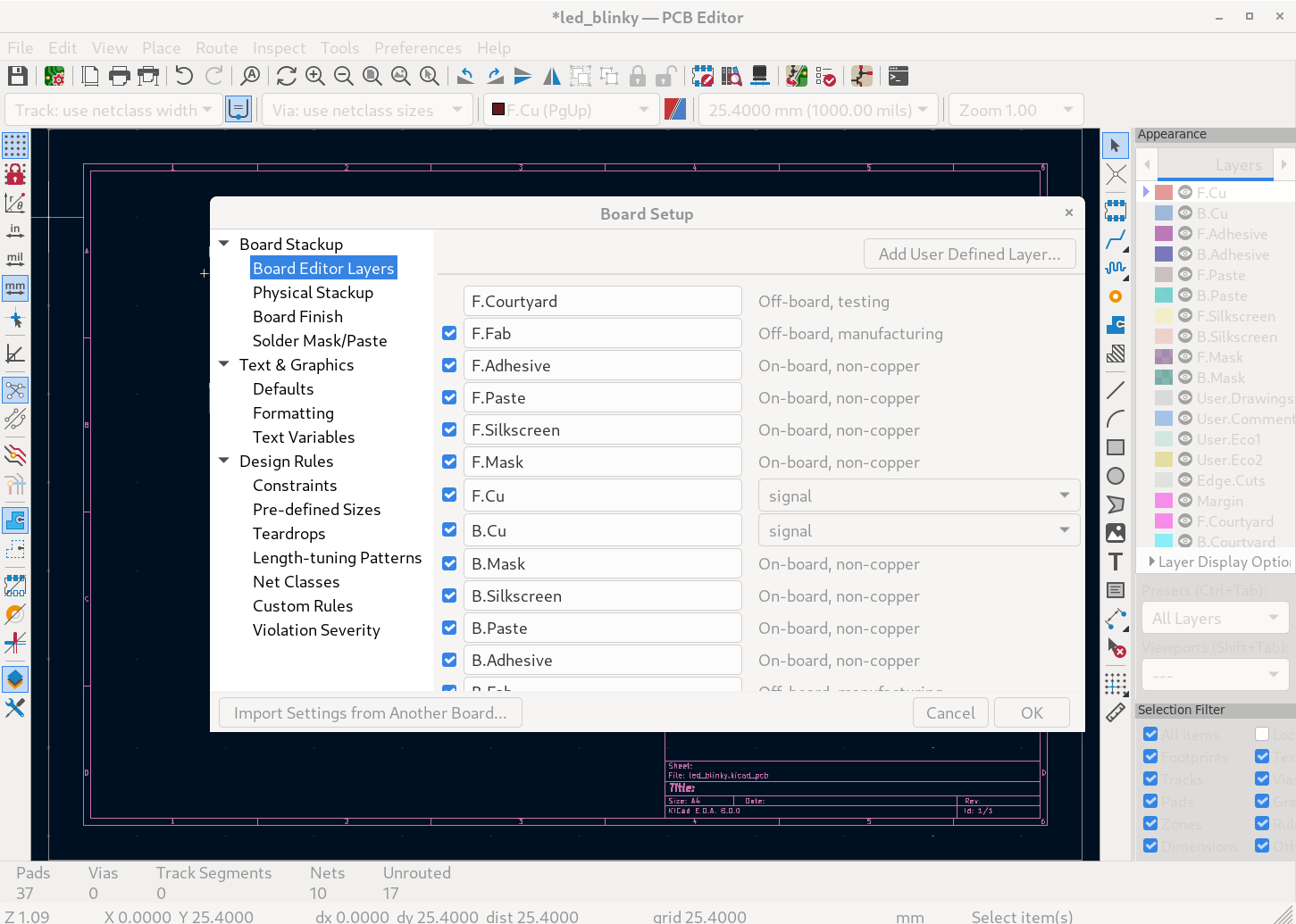
In the Board Editor Layers sub dialog, we can see all the different layers that we can access in the design.
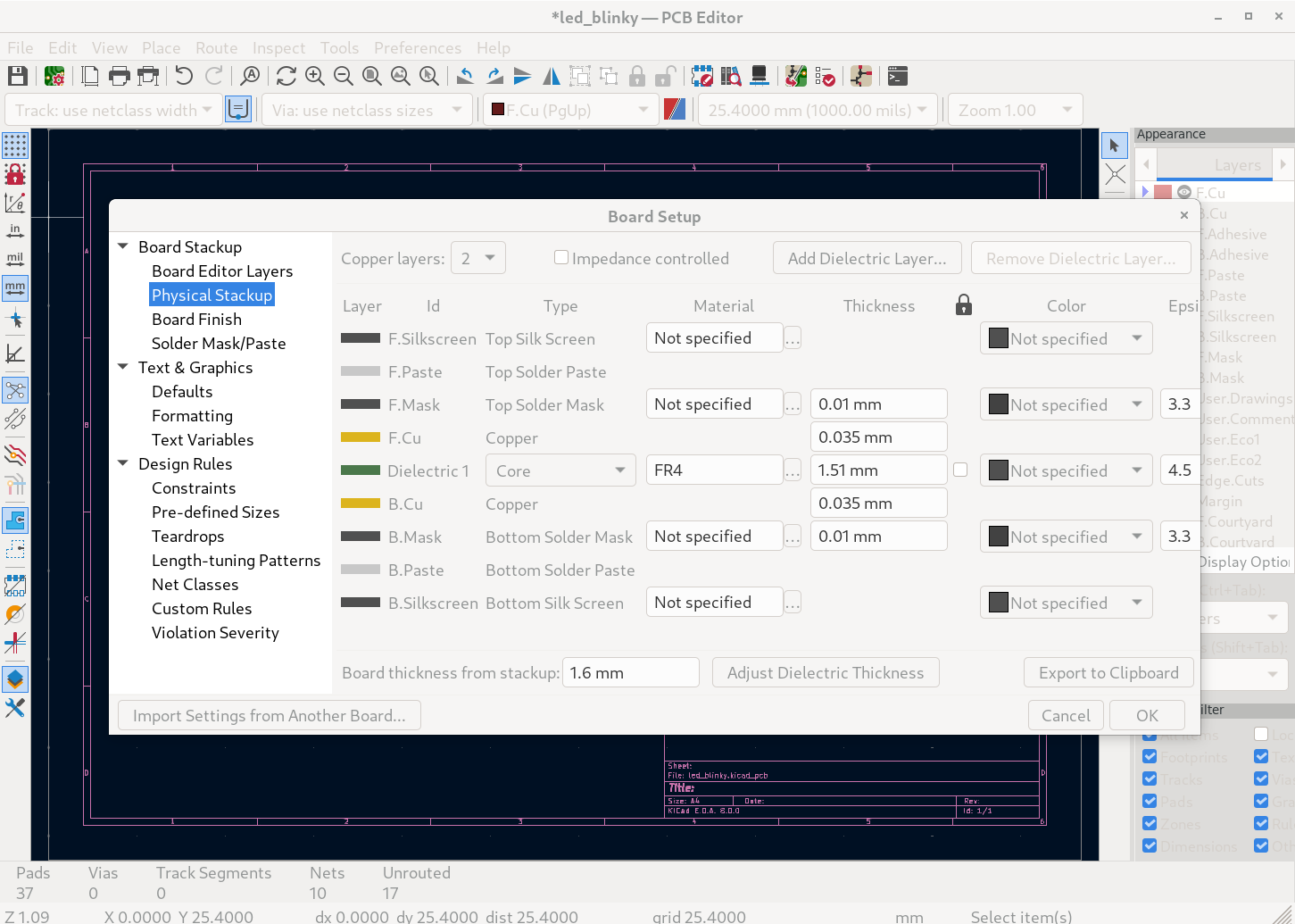
In the Physical Stackup sub dialog we can select the number of layers in the board. Two is the default, and we will leave that as is. You would need to change this value if you want to build a 4-12 layer board.
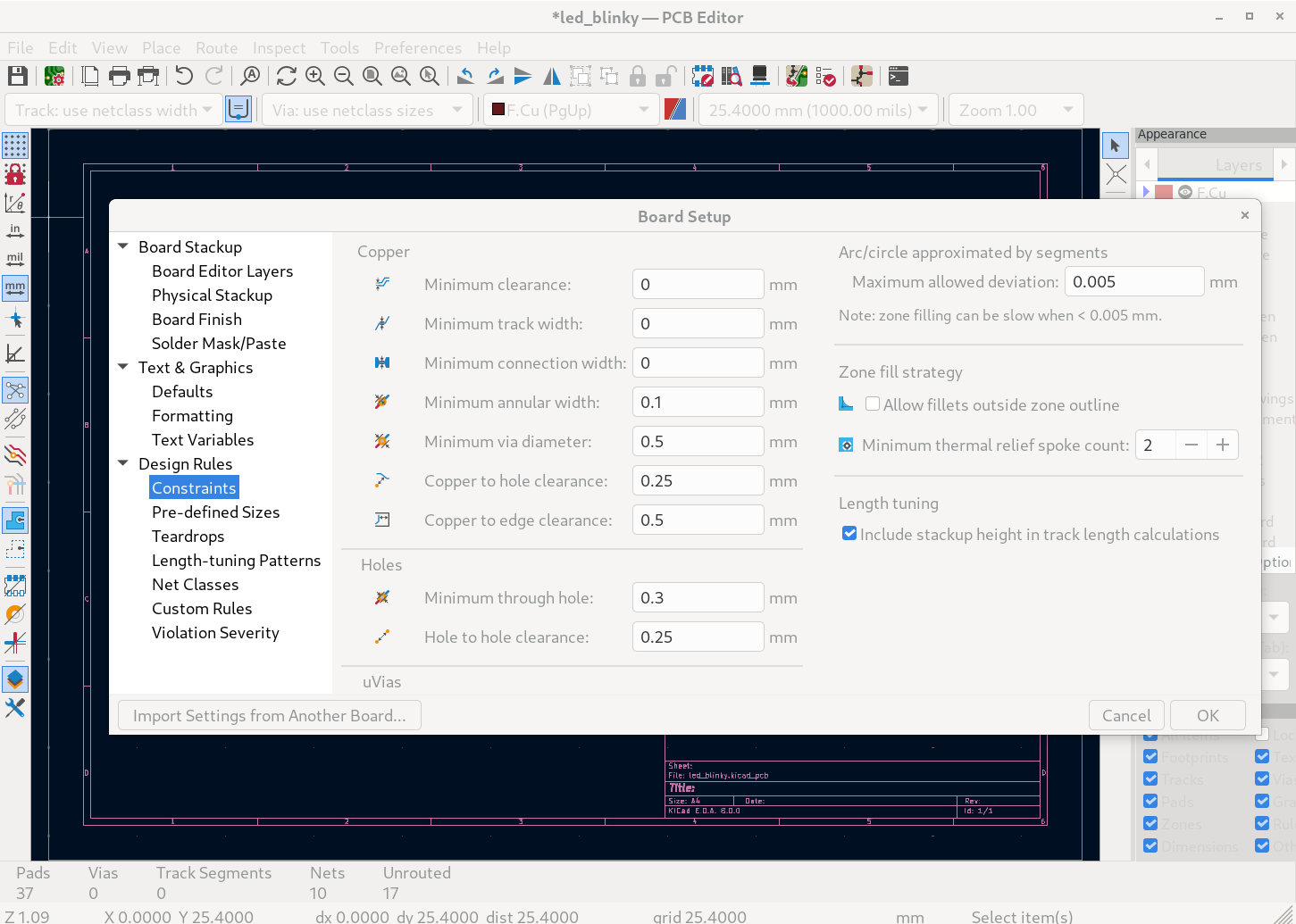
In the constraints sub dialogs we have KiCad’s default design rules. These can be modified to meet PCB manufacturing house requirements. The default rules are adequate for our purposes. So leave them as is for now.
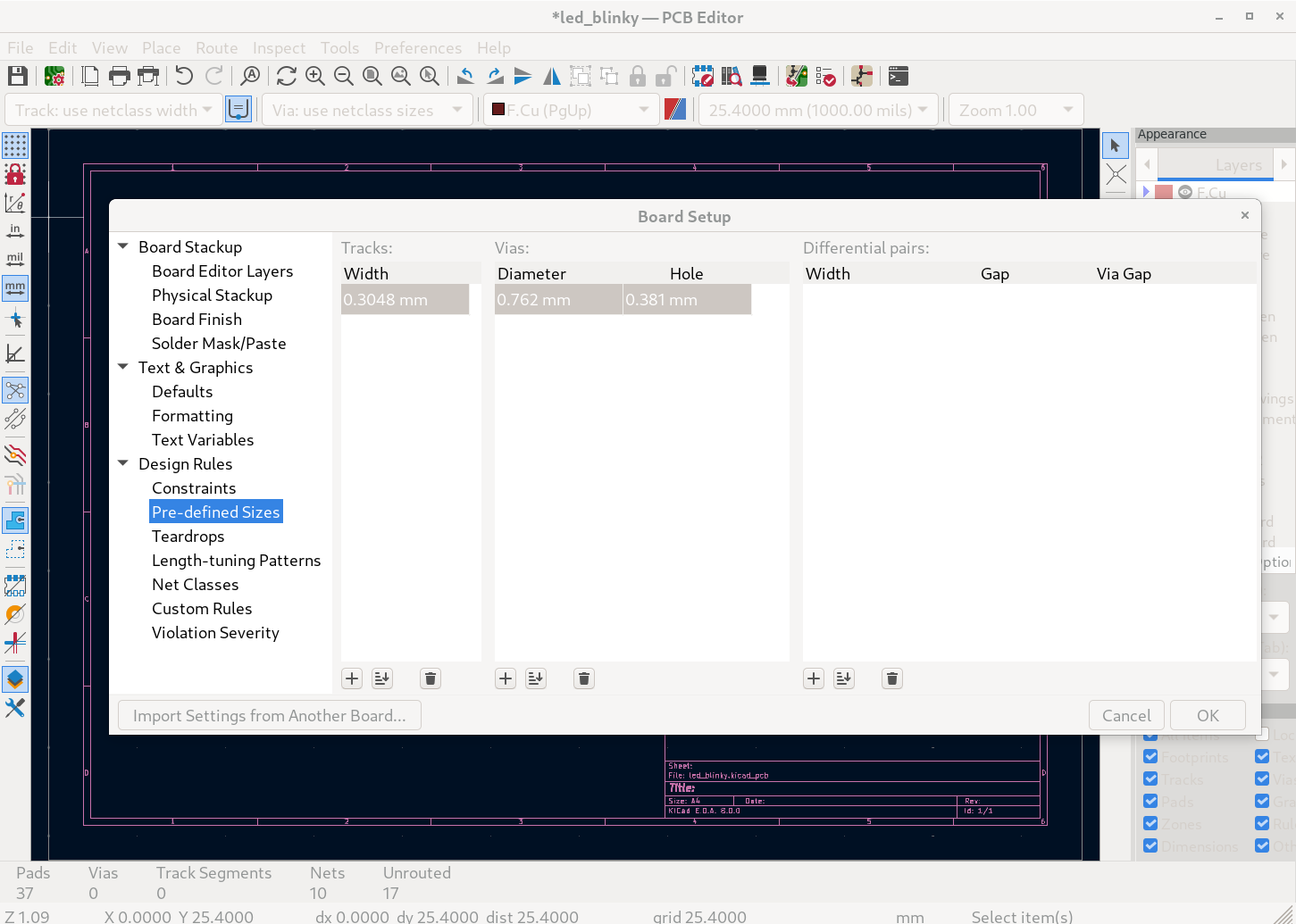
In the Pre-defined Sizes sub dialog, custom trace widths and via dimensions can be specified. Let’s add a custom trace size of 12 mils (0.3048mm) and custom vias size of 30 mil (0.762mm) and hole of 15 mil (0.381mm). This will now show in the drop down menus beneath the top toolbar in the main KiCad layout editor window.
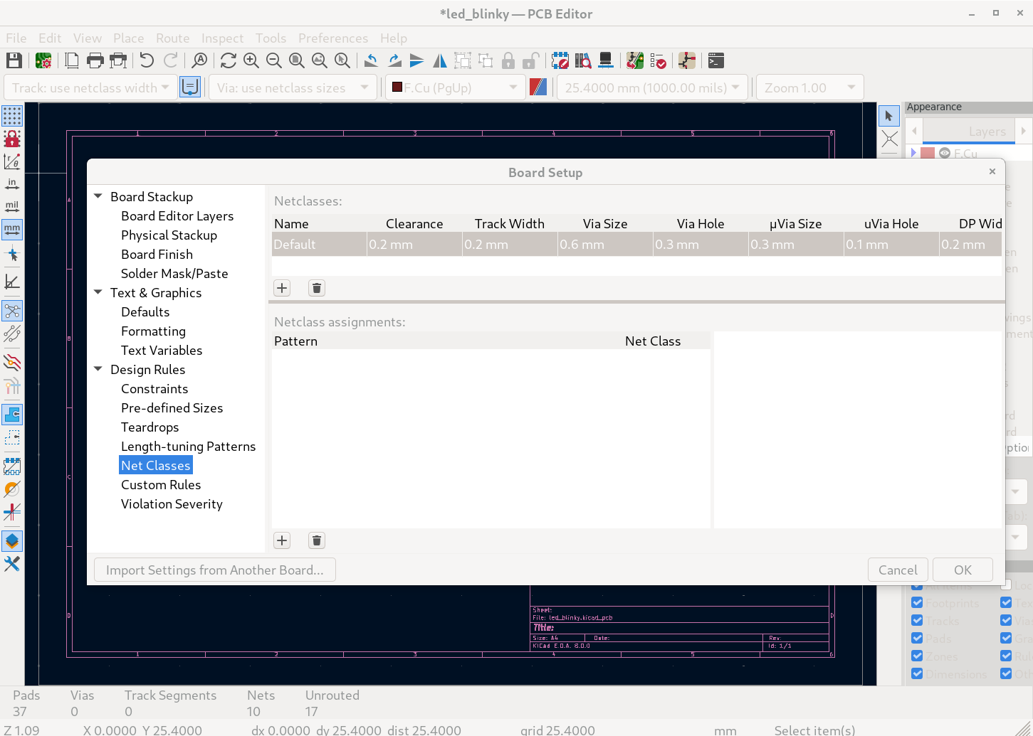
Finally, in the Net Classes sub dialog, we can assign Nets (wires in our design) to Net classes with distinct trace widths. This will come in handy in future designs where we may want to have traces with different widths (to handle different currents; say signal and power net classes) in the same layout.
Click OK to exit the dialog.
Create the PCB Outline
Just like in the schematic editor, the layout editor also has many hotkeys that you ought to familiarize yourself with. The hotkeys list can be accessed via Ctrl-F1 or through the Help menu.
To create a PCB outline:
- Select the Edge.cuts layer from the layer manager on the right hand side of the layout editor window.
- Set the Grid size to 5mm (coarsest metric settings) from the top drop-down menus
- Select the Draw a Rectangle icon on the right toolbar.
- Move the cursor to a location to start drawing the a square 50mmx80mm PCB outline.
- Press spacebar to set the false origin to this same location
- Left click the mouse to start drawing the PCB outline and move down 50mm, and right 80mm, left click again to finish. Alternatively you can use the keyboard arrows to move the cursor. Press enter once to stop.
- Press the Escape button to get back to select mode.
This will give us a rectangular board edge with sharp corners. Ideally we’d like to convert these sharp corners to smoother, ‘more round’ corners. To achieve this;
- Select the board edge and right click. A the context menu will pop-up.
- Choose Shape Modification -> Fille Lines. A tiny Fillet Lines dialog will pop-up.
- Change the fillet radius to 5mm and press OK. The corners should now be round as shown in Figure 10.
Placing Mounting holes and Components
Mounting holes should be included in all PCB designs. They also ought to be integrated in the PCB layout as early as possible. Be sure to set the grid size to a finer setting; say 0.25mm.
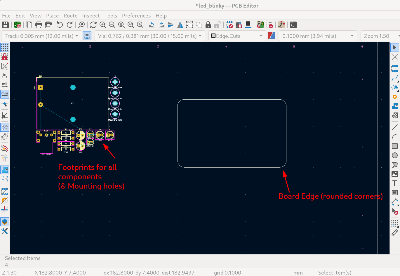
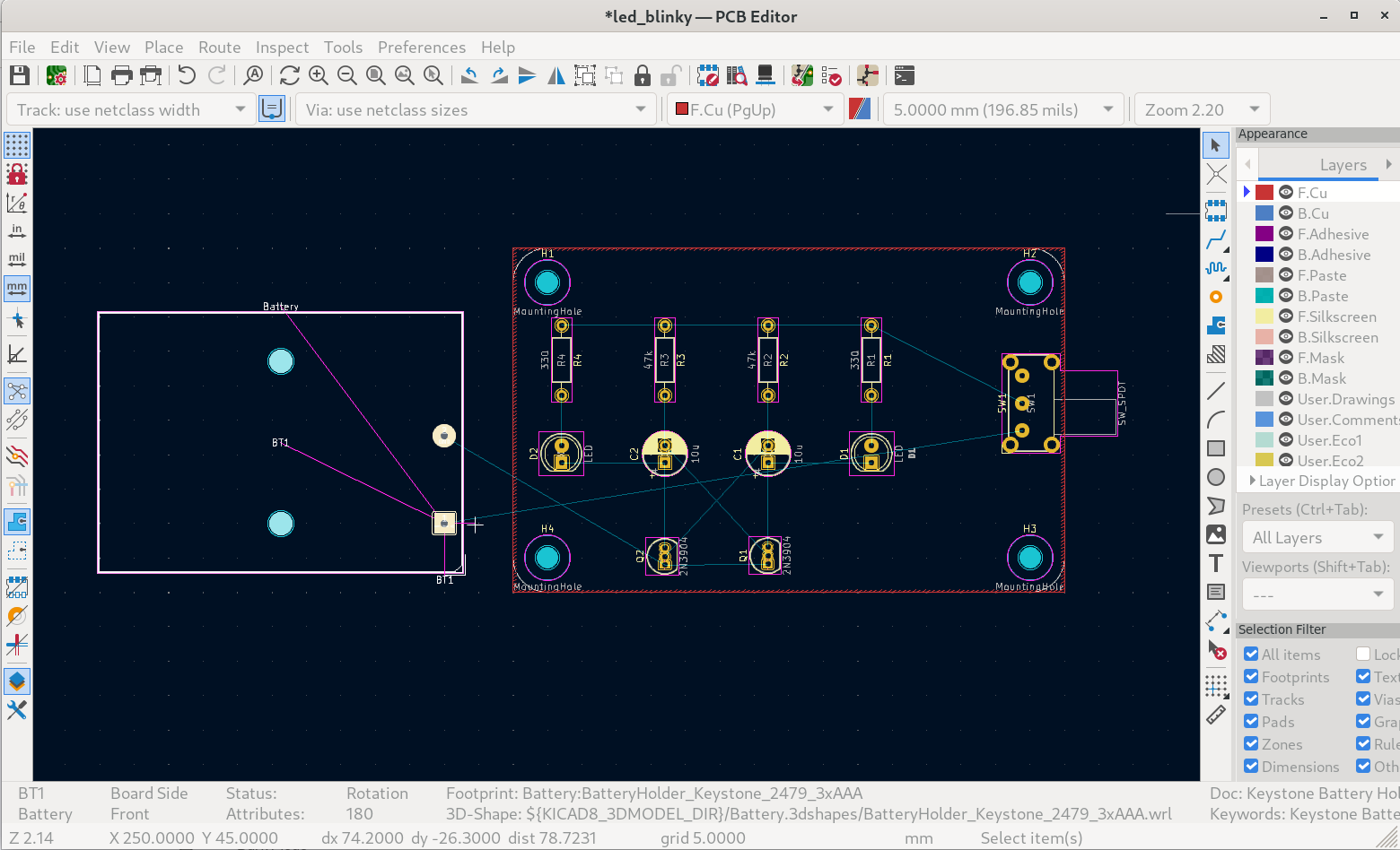
For this particular board, place one mounting hole close to each corner on the PCB outline as shown in Figure 11. Try to make the placement as symmetric as possible (use the grids!!).
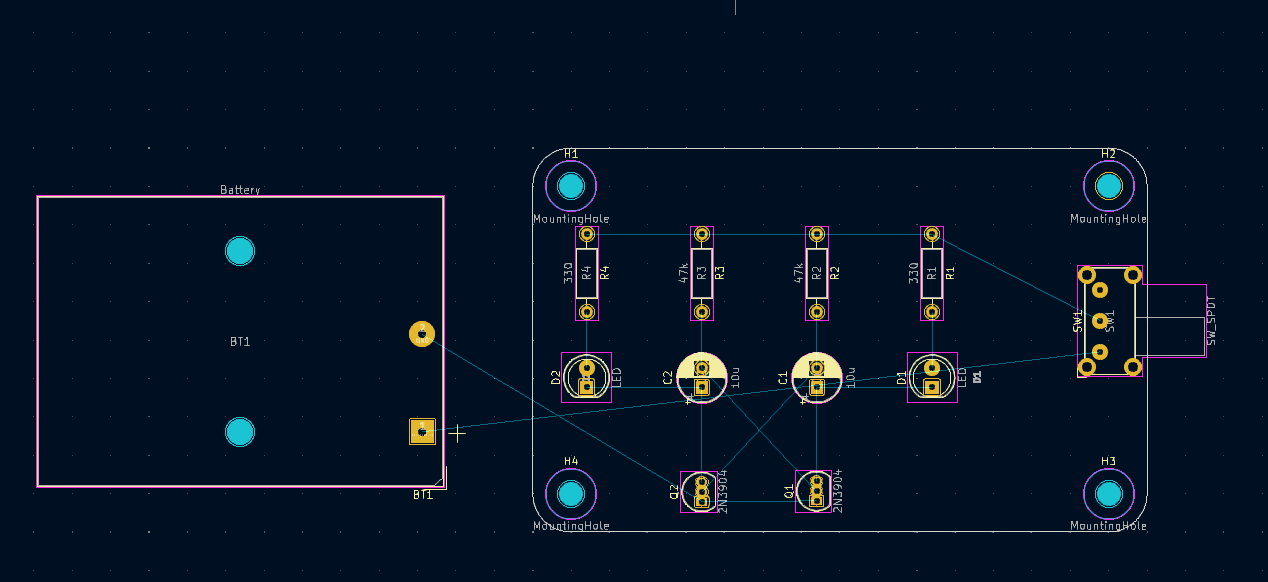
To place components on the board, simply move them over into the PCB outline area. Move all components excluding the battery holder into the PCB outline. You can use the context menu or the m hotkey. The battery holder will be placed last, since it will be mounted on to the bottom of the board. To achieve this, press the f hot key to flip it. Notice how the silkscreen switches colour from yellow (top silkscreen) to pink (bottom silkscreen)
Parts placement is one of the most important steps in layout design. Putting some thought into how each component is placed relative to other components will help reduce routing conflicts and make the trace routing step (next step) much easier.
If two components are connected directly to each other in the schematic, be sure to place them as closely as possible in the layout in a way that minimizes the criss-crossing of the ratsnest lines (white lines connecting footprints together…more on this in the next paragraph). One possible placement is shown in Figure 11.
Add Two Ground planes
Printed circuit boards can have from 1 to more than 50 routing copper layers. I like to have a minimum of 2 layers for simpler designs like this one. Two layer boards allow the designer to route traces between components on the front copper layer (top side of the board) as well as the back copper layer (bottom side of the board). In fact, one can start a trace in one layer, use a via to switch over to the other layer and continue to draw the rest of the trace on this new layer!. But what do we do with all the board real estate on both layers that is not used by traces or vias?
A ground plane is created by assigning all the unused copper fill (portions of copper fill not used for traces/pads/vias) on both top and bottom layers to the ground net. This has the following advantages:
- Reduces noise
- Improves signal integrity.
- Because the ground net is available almost everywhere on the board, ground trace routes may not be needed, reducing the complexity of the trace routing procedure.
In most 2 layer designs with traces, the goal is to route as many traces as possible on the top layer along with a top ground copper fill that covers the unused areas. Traces are routed on the bottom layer only when necessary, allowing as much as possible of the bottom layer to be utilized as a contiguous ground fill/net. Since our design is relatively simple, we should use only the front (top) layer for trace routing. And assign ground copper fills ( or planes) to both the back (bottom) layer, and the unused portions of the front layer.
To add a ground plane,
- Set the Grid size back to 5mm (coarsest metric settings) from the top drop-down menus
- Select the Add a filled zone icon from the right toolbar or use the hotkey Ctrl-Shift-Z.
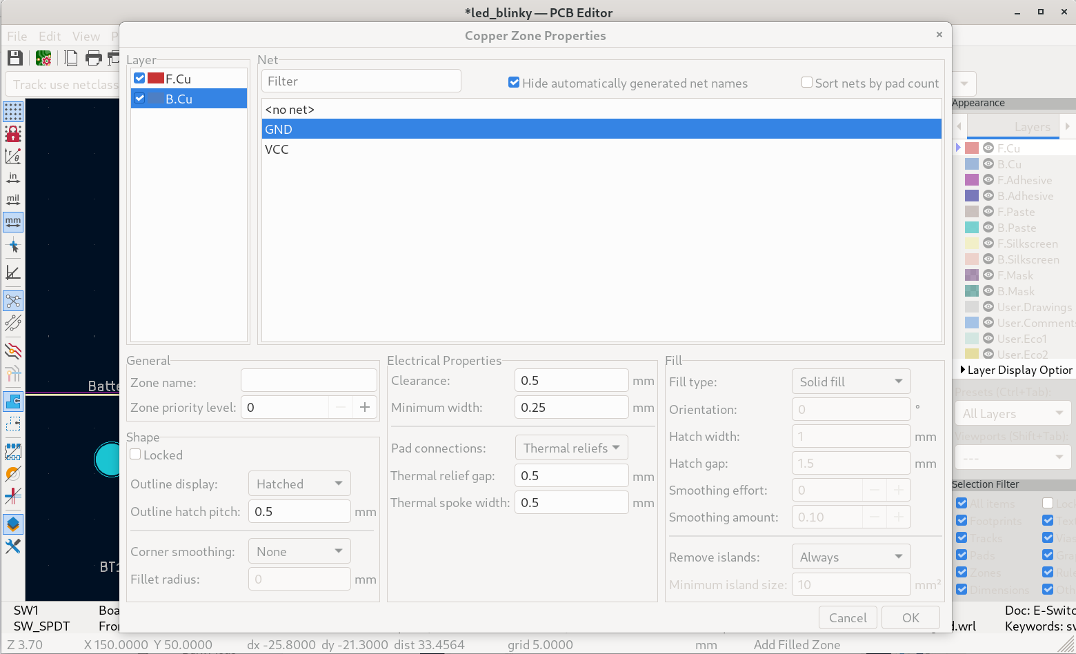
- Place the cursor on the top left corner of the PCB outline and left click the mouse. You will be greeted with a Copper Zone Properties dialog.
- Be sure to select both the front copper (F.Cu) and bottom copper (B.Cu) layers and the GND net as shown in figure 13. Then press OK. Move the cursor to all four corners (follow the same path as that of the PCB outline) on the board to successfully place the ground plane.
Route Traces
The blue lines connecting the footprints to each other in Figure 13 are called the ratsnest. They indicate where the copper traces need to go to connect the components as per the schematic (netlist). This process is called manual routing when done by the PCB layout designer. Routing can also be done automatically (autorouting) by a computer algorithm, but in many cases the designer will want to route traces manually. To route these traces manually click the Route tracks icon from the left toolbar or use the Shift+x hotkey.
Always be sure to exit or enter pads (end routes) at the N, S, E and W points. Avoid diagonal routes leaving from or entering to the pads. Also avoid 90 degree turns in your routes.
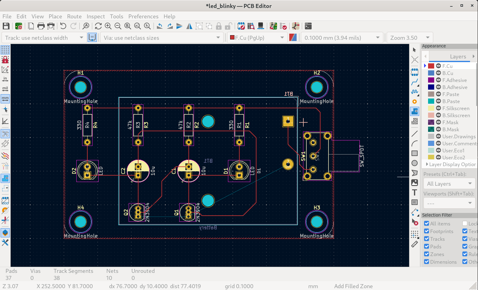
- Set the Grid size back to 0.25-0.1mm.
- Route all tracks (matching the ratsnest) in front copper (F.Cu) only. This process can be tricky. Try doing it yourself and refer to figure 14 only if you need help. Notice that you will not need to route the ground traces as shown in Figure 14.
- Select the battery holder footprint, flip it (if not done so already) so that it’s mounted on the bottom layer by using the ‘f’ hotkey. Then place it as shown in figure 14. Route the traces attached to it. Again you will not need to route the ground net for now.
- Click on Add a filled zone icon again. Move the cursor inside the layout and right click. Go to Zones->Fill All Zones This will fill in the copper fill. The board should now look as shown in Figure 15. If you make any modification to your board i.e. move a trace or part e.t.c., you’ll have to repeat this step again. You can also turn OFF the zones by clicking on the Show only zone boundaries icon in the left toolbar.
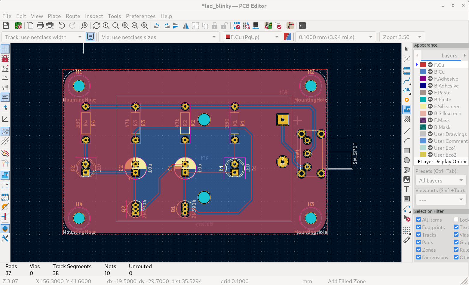
Notice that the ground pins on the transistors and the battery holder are connected directly to the ground copper fills via spokes. These spokes are called ‘thermal reliefs’. It can be hard to get solder to reflow on pads that are directly connected to copper fills because the heat dissipates across the entire copper fill. Thermal reliefs allow us to have our cake and eat it too; i.e.provide a robust electrical connection from the pad to the copper fill, while preventing the heat needed for soldering from dissipating into the copper fill.
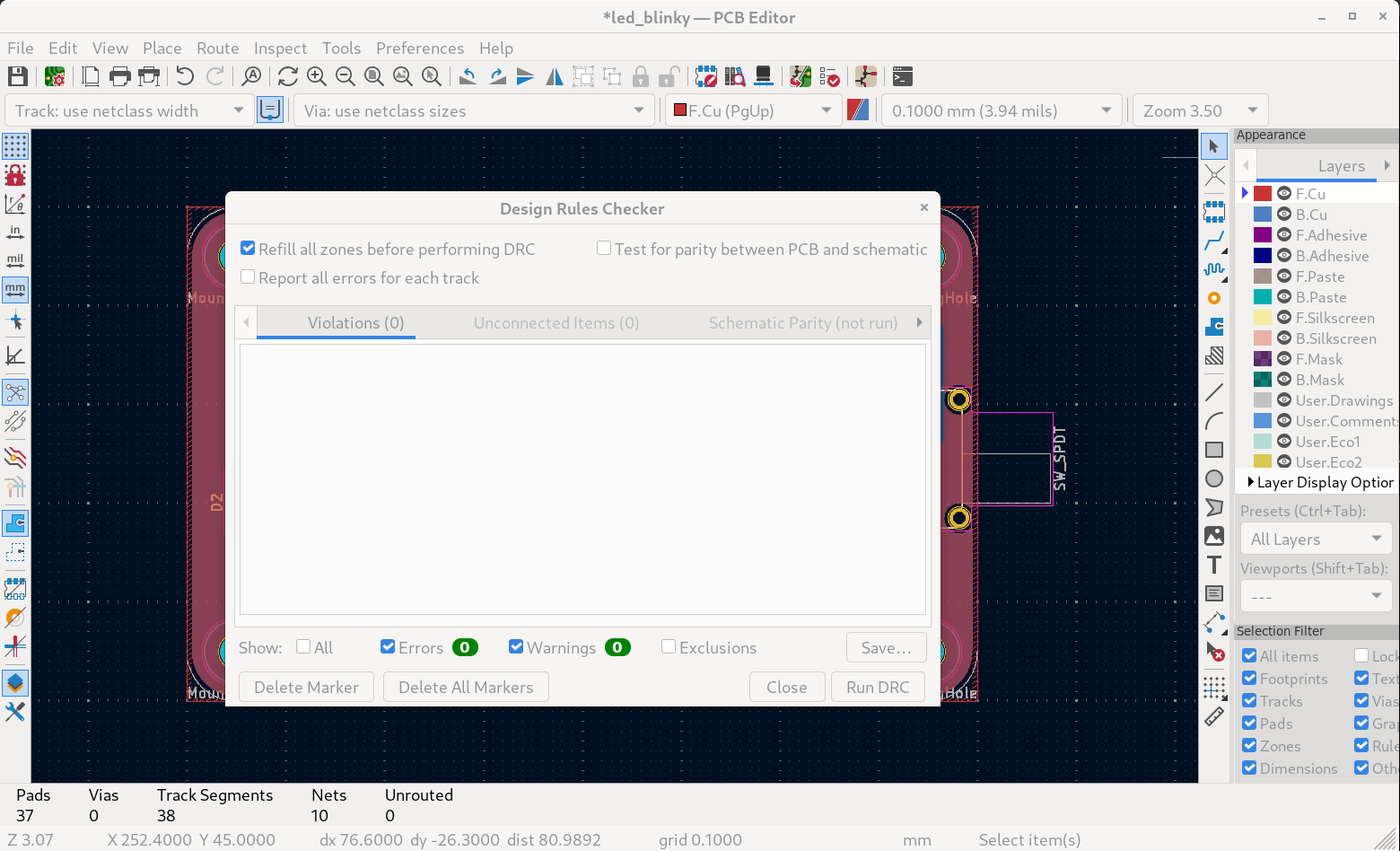
Design Rule Check
In order to verify that the PCB layout has so far respected the design rules, run a design rule check (DRC). This can be accomplished via Inspect->Design Rule Checker. This opens the DRC Control dialog. Then click on the Run DRC button shown in Figure @fig:18.
Any problems listed under Violations must be rectified. Also the Unconnected Items should be zero, if its more than zero, this indicates that you forgot to route some of the traces.
If the DRC passes without any problems and no unconnected nets, then congratulations! The layout is valid and almost complete!.
Add Text & Logo
To add text to the Front silkscreen, select the Add a text item icon in the right toolbar Ctrl+Shift+T and left click in the layout area. In the resulting dialog, write in the Text field the text to be displayed on the board. Be sure to select the front silkscreen layer (F.SilkScreen) to write text in the front silkscreen layer. The text’s size and position can also be adjusted from the very same dialog. Once you are happy with the text, simply press the OK bottom and move the text to the appropriate location on the board.
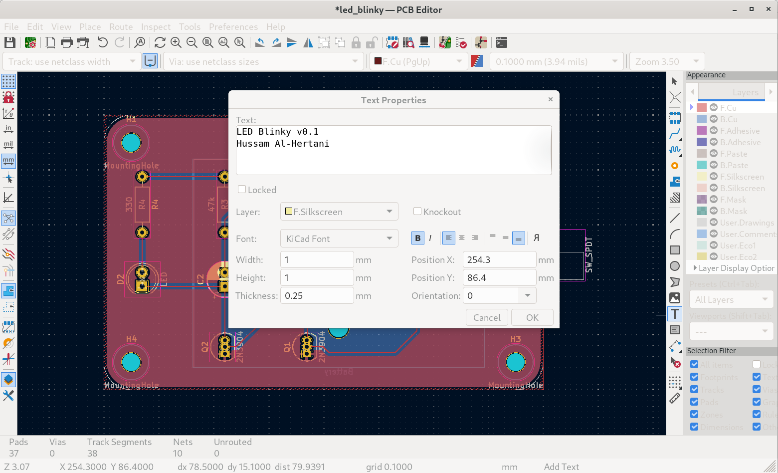
Be sure to add your name and the name of the design on to the board. Also add ON/OFF labels for the switch positions as shown in Figure 18.
Adding a logo is a little bit more complicated. KiCad can convert logo images into a footprint that can then be added to the footprint libraries. The complete process is listed below:
- First create three nested folders in your root folder KiCadProj called myLibraries/myFootprints/logos.pretty.
- The myLibraries folder will contain all custom schematic symbol and layout footprint libraries that you may decide to create in the future.
- The myFootprints folder will contain all future custom layout footprint collections
- The logos.pretty is the folder that will contain all custom layout footprints that are logos. Notice that layout footprint collections must be placed into folders with a .pretty extension.
- From the KiCad main window select Image Converter.

- Choose a reasonable logo image that is sized around 256×256 pixels. Logos will show up better on the PCB if they are less complicated. Avoid photos. For the sake of this exercise, use the smiley logo shown in Figure 19.
- Once the Image Converter application opens, load the logo into the application through the Load Source Image button.
- Be sure to set Format: to Footprint(.kicad_mod file) and Board Layer for Outline to Front silk screen
- Set the Size to 20 by 13.3mm and the Black/white threshold to 70.
- Press the Export button and save the file as smiley.kicad_mod in the logos.pretty folder (Figure 21).
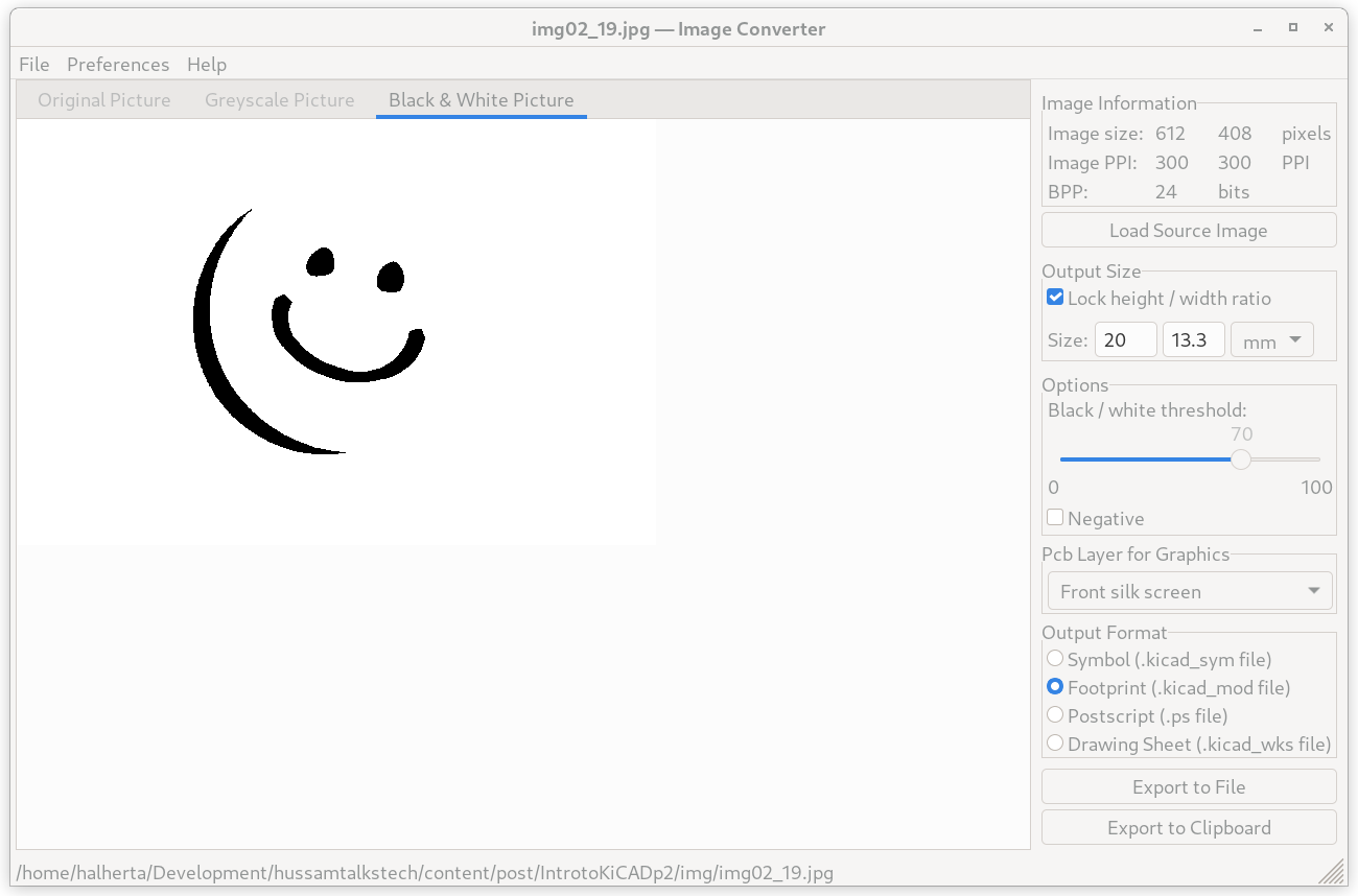
The goal is to always have the image features be dark on a white background. If that’s not the case, experiment with the negative checkbox and the Black/white threshold slider.

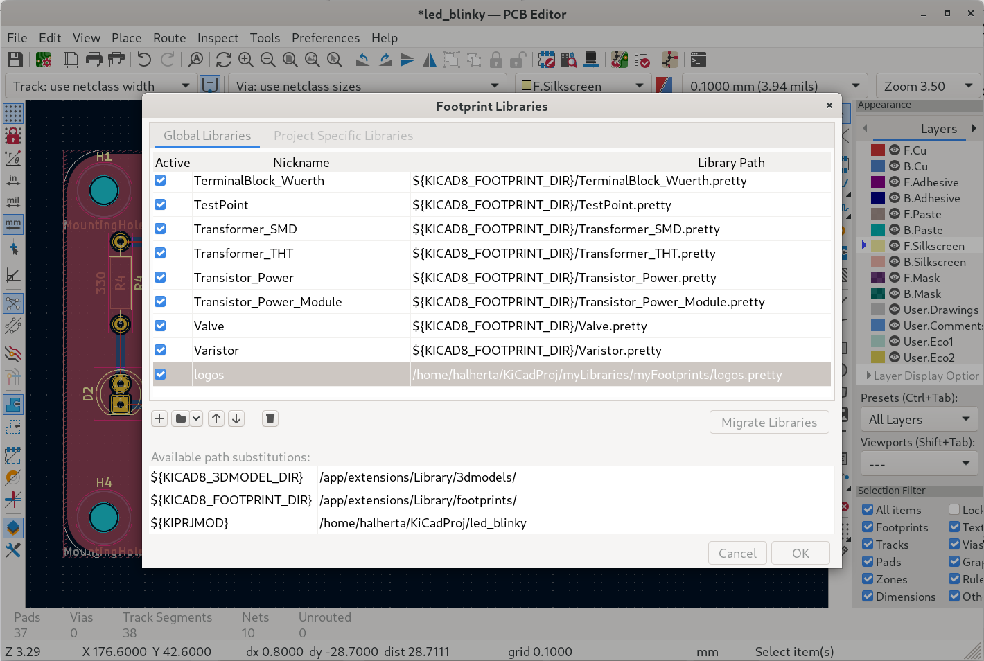
- In the PCB Editor, go to Preferences->Manage Footprint Libraries
- Select the Global Libraries tab
- Press the Add existing library to table button (folder icon) and enter a name for this library and its library path as shown in Figure 22.
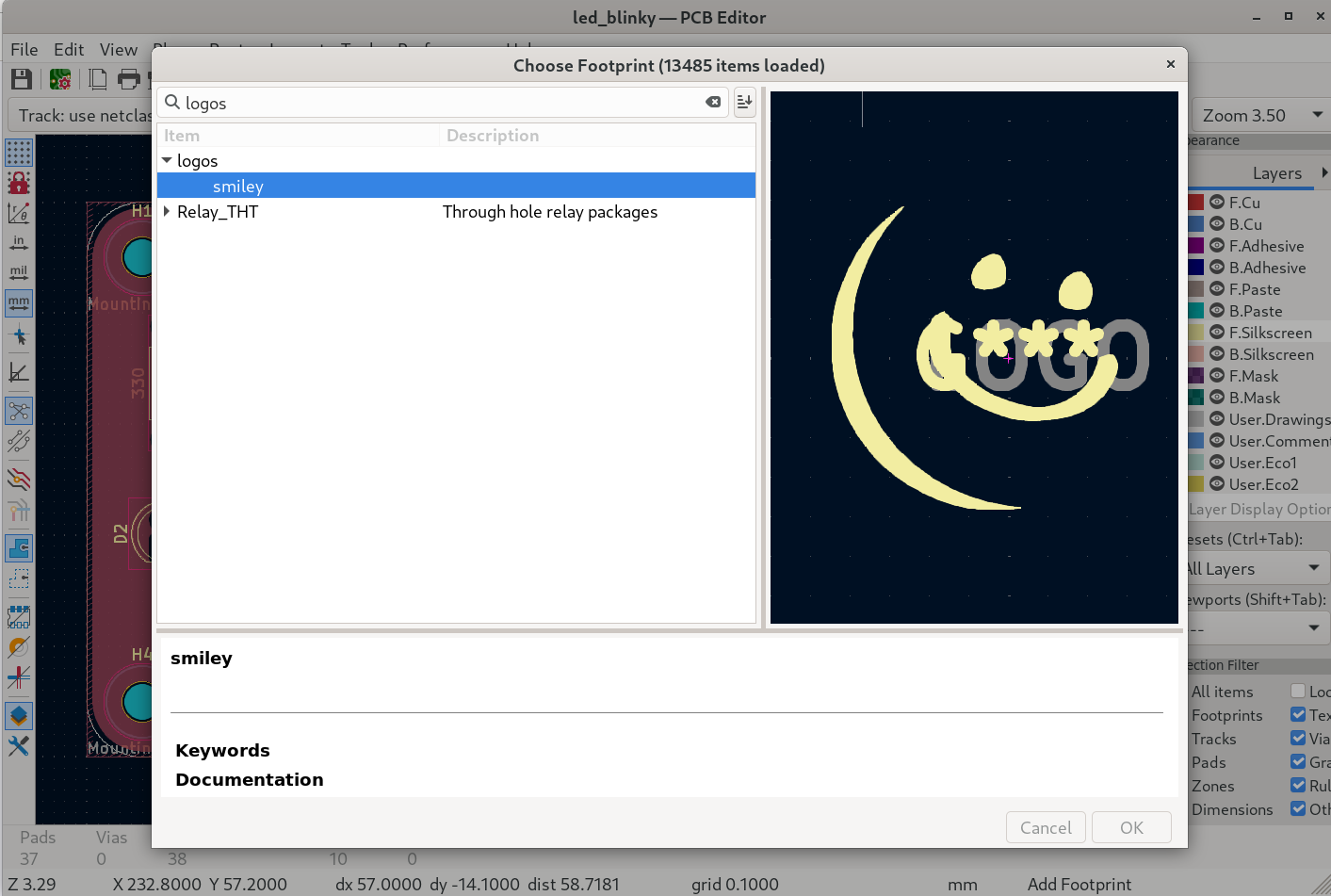
- In the PCB ditor, select the Add Footprint icon (hotkey is a), then left click anywhere within the layout editor’s grid area. This will open a Choose Footprint Dialog.
- In this dialog go to the logos library on the left-hand side and double click on the smiley footprint as illustrated in Figure 23.
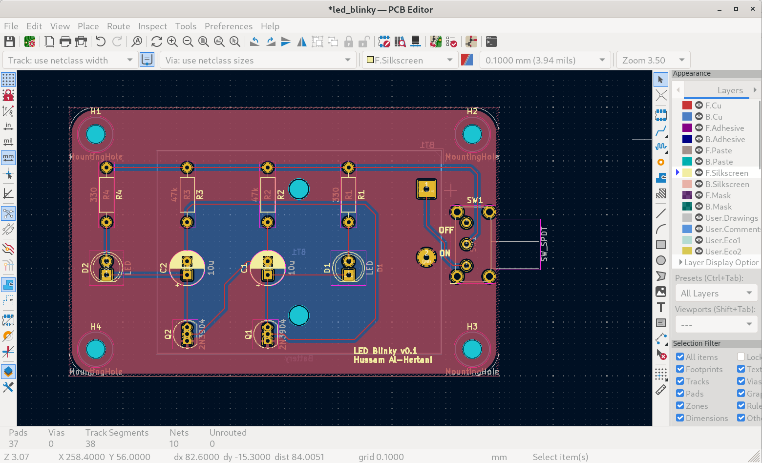
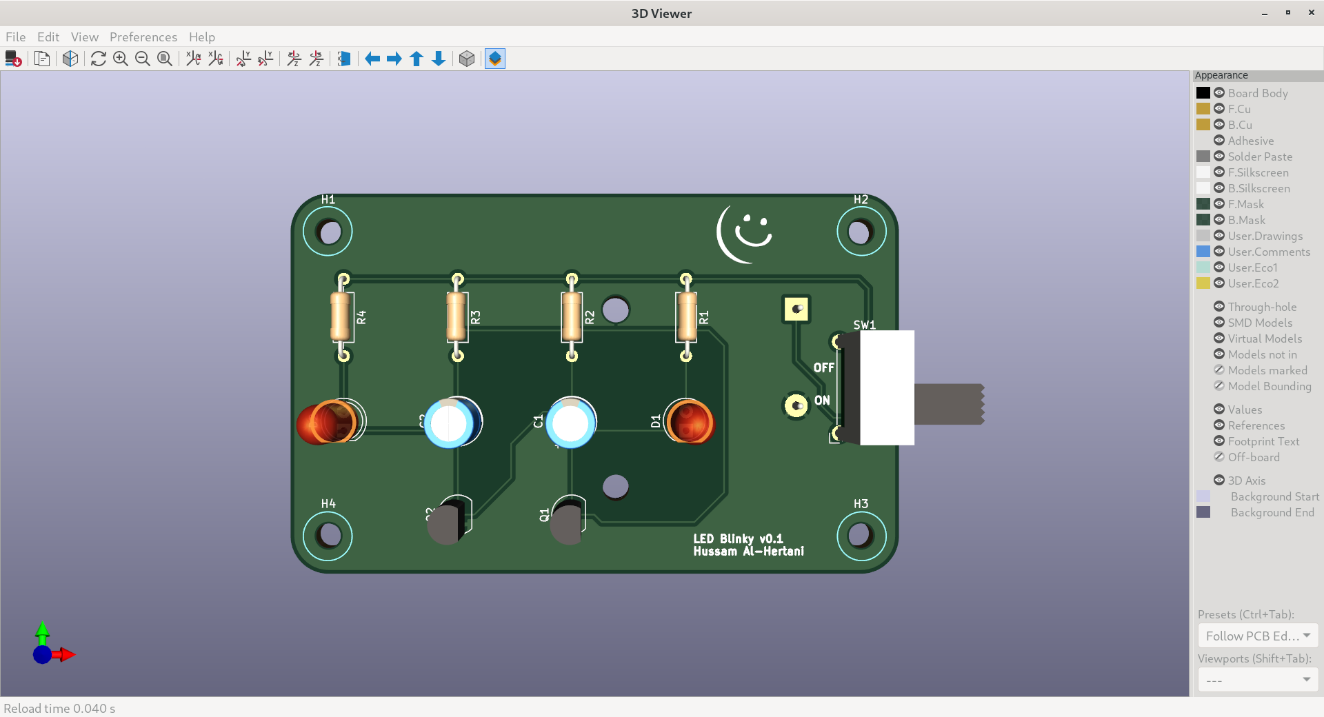
- Now place it in the PCB layout. You’ll notice a G** * reference value is visible. If you select the logo and press the ‘E’ hotkey (or right click -> Properties), you can render the reference value invisible. The final layout with filled ground planes is shown in Figure 24.

KiCad’s PCB Editor also comes with a 3D viewer. To access it, go to View->3D Viewer. Figure 25 illustrates what the board looks like in the 3D viewer.
Generate Gerber files
In order to fabricate a PCB based on our layout , the layout’s Gerber files need to be generated. Gerber files contain information about the location and contents of each layer i.e. Front Copper, Front Silkscreen, Drill holes. e.t.c
To generate the Gerber files:
- Create a directory called Gerber in your project directory
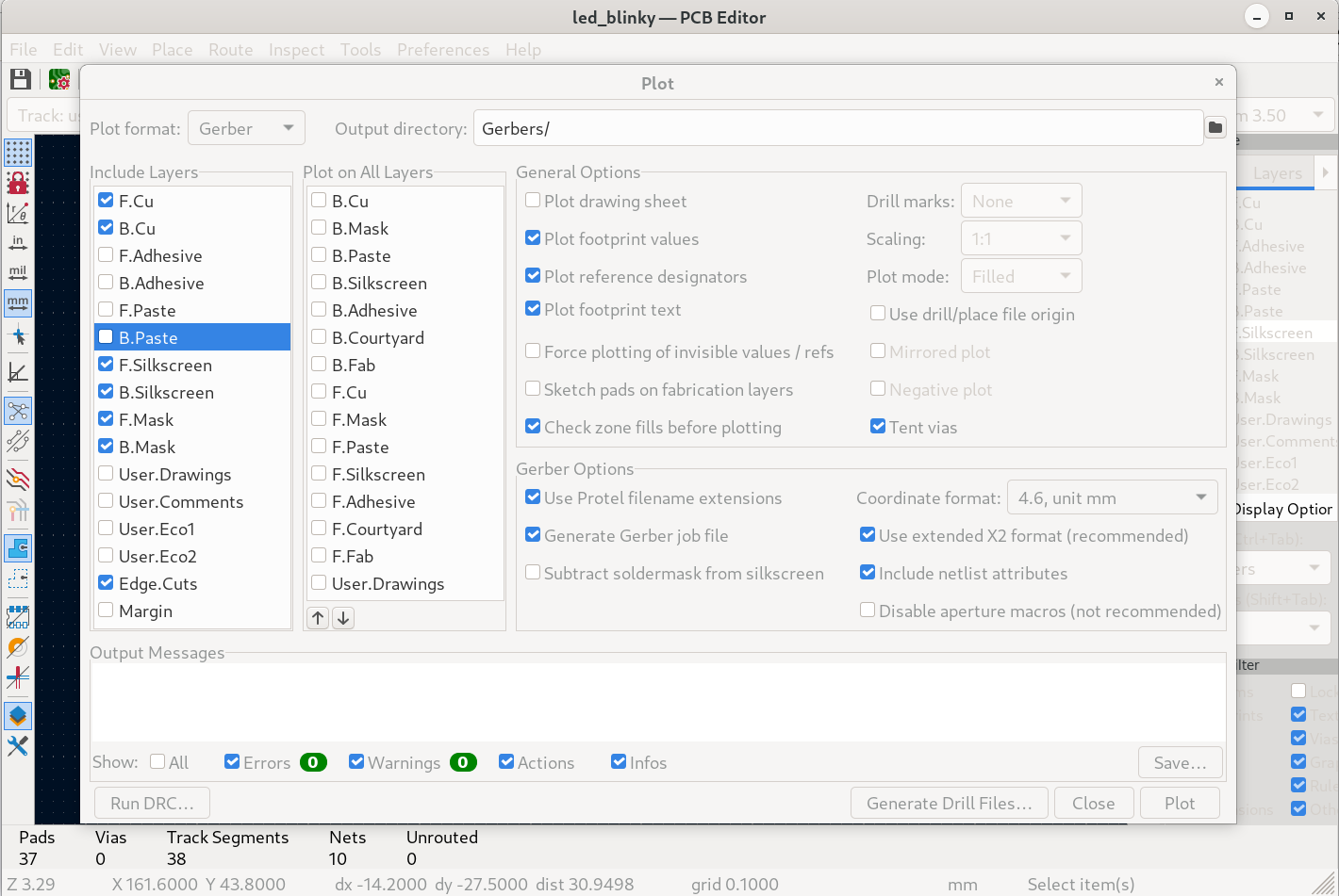
- Select File->Plot from the top menu.
- In the plot dialog be sure to select the 7 layers shown in Figure 26.
- F.Cu (.gtl) -> Front/Top Copper
- B.Cu (.gbl) -> Bottom Copper
- F.Silkscreen (.gto) -> Front/Top Silkscreen
- B.Silkscreen (.gbo) -> Bottom Silkscreen
- F.Mask (.gts) -> Front/Top Soldermask
- B.Mask (.gbs) -> Bottom Soldermask
- Edge.cuts (.gm1) -> Board Edge
- Under Gerber options select Use Protel filename extensions as shown.
- Set the Output folder to Gerbers and press the Plot button. This will create all the necessary Gerber files (except the drill file) and place them in the Gerbers folder within the project folder.
To generate the drill(.drl) file:
- Press the Generate Drill files… button in the Plot dialog. This will open a new dialog called Generate Drill Files.
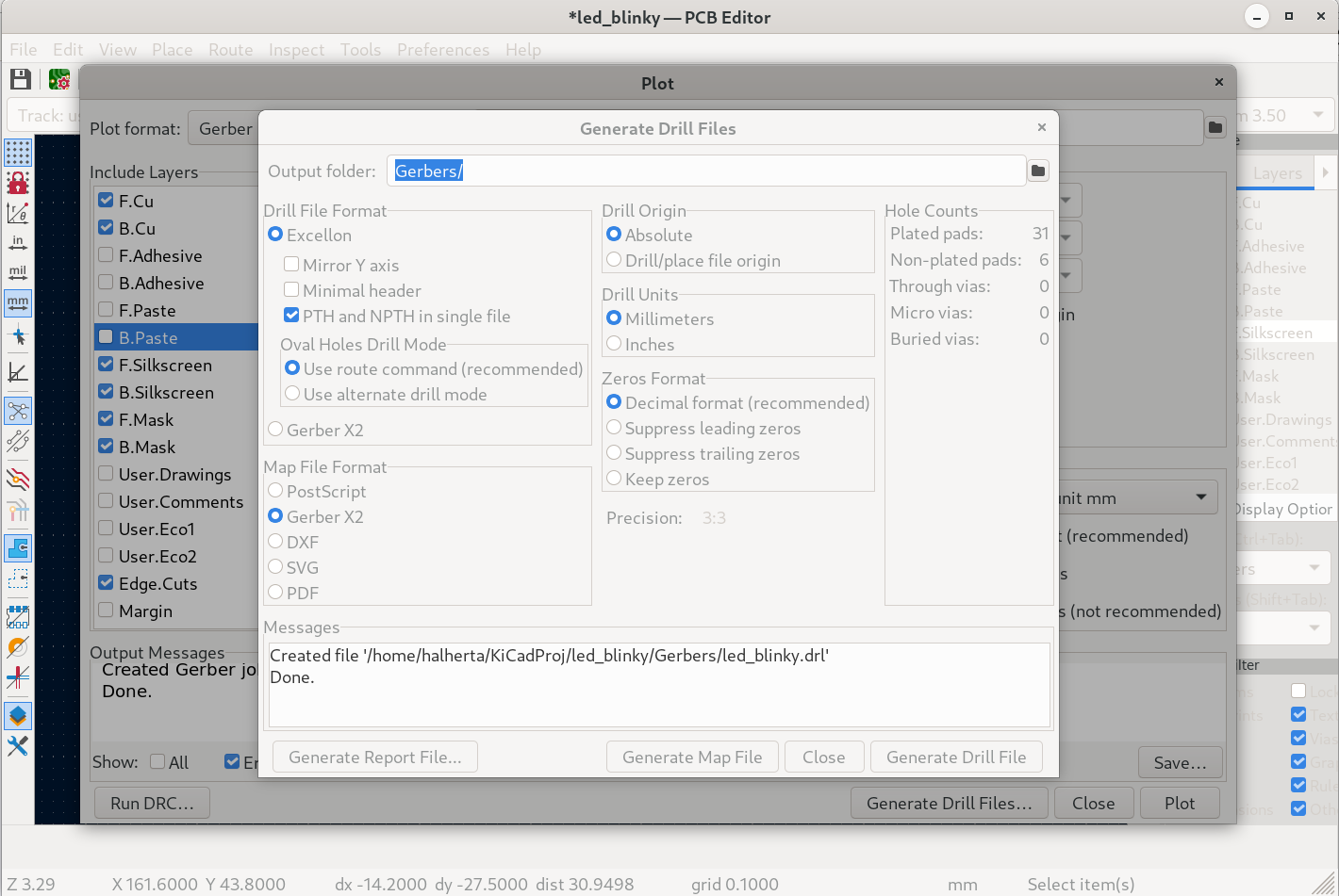
- In this dialog, be sure to set the Drill Units to Millimeters.
- Under Drill File Format, select Excellon & PTH and NPTH holes in single file.
- Be sure to set the Output folder to the path of the Gerber folder created earlier
- Press the Generate Drill File button
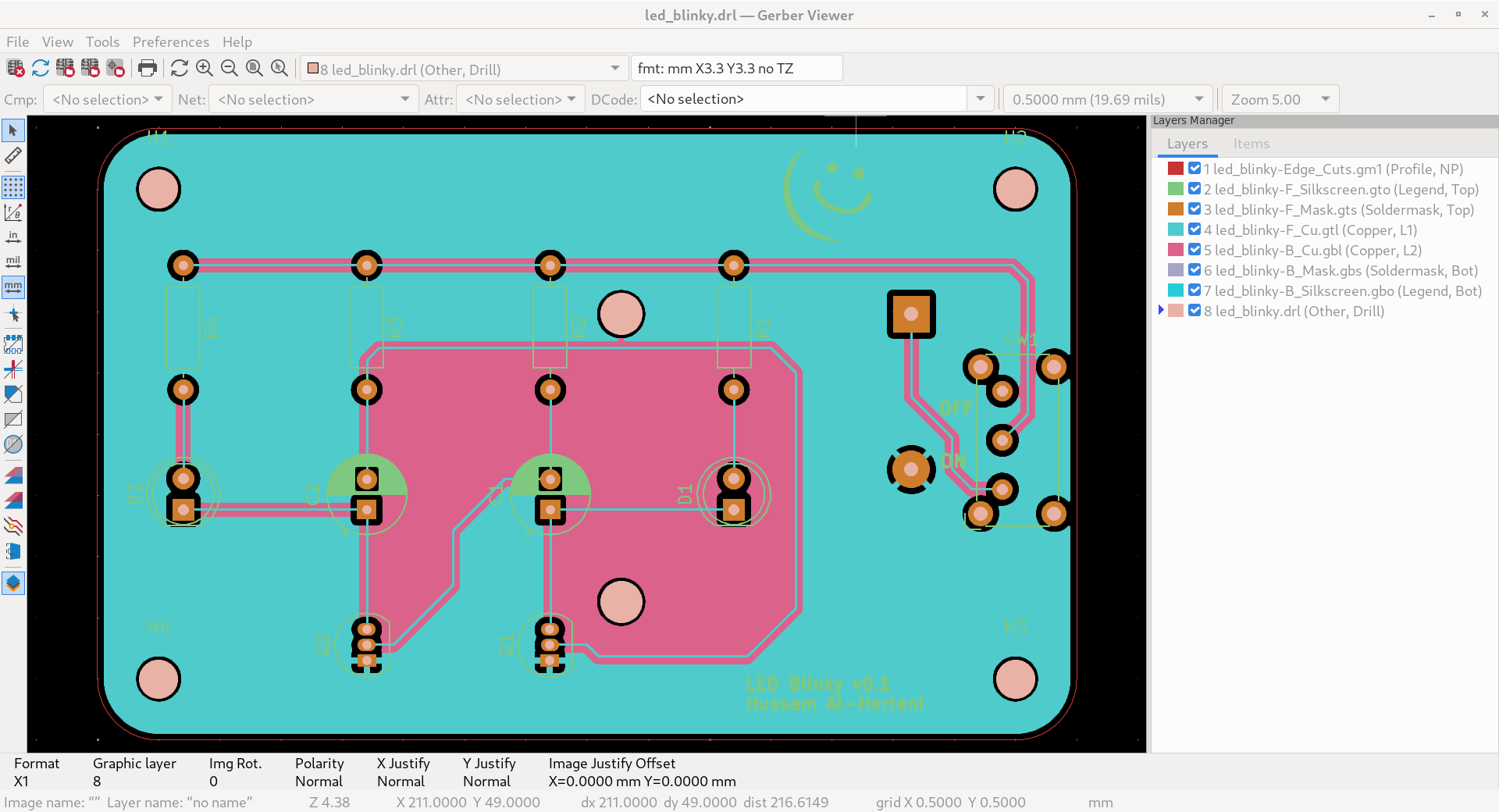
- The Gerbers folder now holds all necessary files for fabrication!
- You can now view the Gerber files and drill file in the Gerber viewer accessible from the main KiCad window.
And that’s it! Compress the Gerbers folder into a zip file and upload it onto your favorite PCB manufacturer website. I’m making the entire KiCAD project available for download from my github. This has been a rather long entry. My goal is to make this tutorial available in a video format in the near future.
Thank you for this tutorial, it has been extremely helpful!