
The objective of the IoTIS ecosystem is to provide a standardized platform for students to develop their capstone projects. The baseboard and the powerboard are typically made available to all students. The students would then have to build their own Arduino shield-compatible daughterboard; which is application-specific to their particular capstone project and its requirements.
The layout of the Arduino shield-compatible daughterboard is part of these requirements, and students are solely responsible for the layout of their daughterboards, except for their outline & pin spacing. Just like with the baseboard and powerboard, the daughterboard is also made available as a template. A schematic symbol for the daughterboard is made available (see schematic in Figure 2).
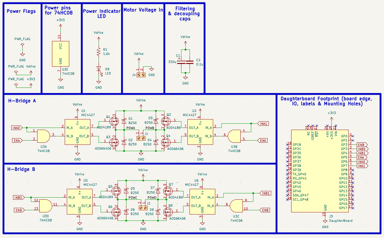
This symbol pulls in the daughterboard outline footprint shown in Figure 3, which includes the board edge, pin spacing, and the pin labels. The students need only build their application-specific circuit schematic and attach its inputs and outputs to pins on the daughterboard symbol in their schematic.
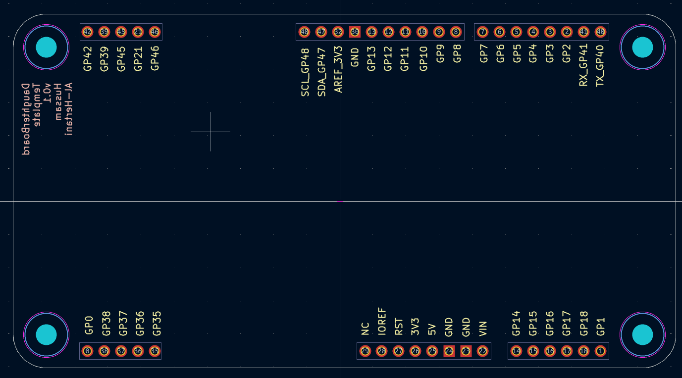
The students can also utilize the +3V3, +5V, and VIN rails that are made available on the daughterboard schematic symbol via the baseboard and powerboard. For circuit designs that need additional power rails, like the motor voltage rail ‘Vdrive’ required by this H-bridge design, they can always add additional pins or terminal blocks on the daughterboard to bring in this additional rail directly. In this particular design, the motor voltage rail ‘Vdrive’ is brought in via block terminal J4.
Motor controller circuit design philosophy and considerations
This particular daughterboard design was developed as a reference design to motivate students and walk them through the process of creating a PCB layout in this form factor.
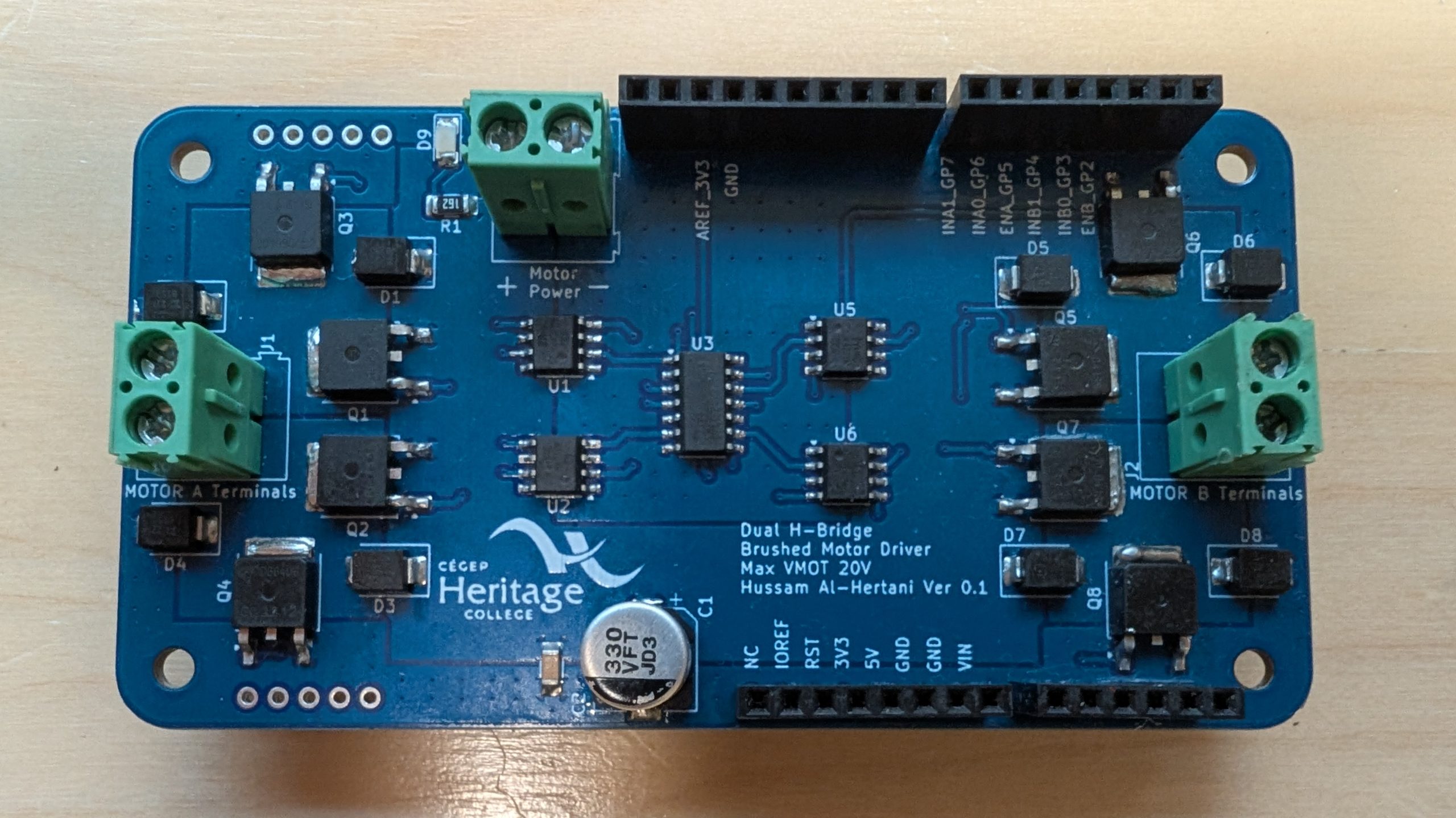
The motor controller circuit consists of two MOSFET H-bridges intended to control one brushed DC motor each. The circuit is rated to run at a maximum of 16V and deliver 5-7A of current to the motor.
The H-bridge consists of two P-channel MOSFETs on the high side and two N-channel MOSFETs on the low side. The drains of the P-Channel and N-Channel MOSFETs connect at the POWx nets. The MIC4427 MOSFET driver ICs are used to drive all four MOSFETS.
A downside of this particular configuration is that the maximum motor voltage cannot exceed the VGSMAX rating of the MOSFETs (+/- 20V). We chose to build a margin of error and de-rate the maximum motor voltage of the design to 16V.
INx0 and INx1 directly control the P-channel MOSFETs through the gate drivers and provide high-side control. INx0 and INx1 are also ANDed with ENx before driving the N-channel MOSFETs to provide low-side control. This allows the enable pin (ENx) to ‘gate’ the low-side N-channel MOSFETs.
To control the speed of the motor, one only needs to provide a PWM signal to the enable pin (ENx), which in turn switches the N-channel MOSFETs (low side) while keeping the P-channel MOSFETs (high side) in a static state. Because we are not switching both the low and high side MOSFETs, we avoid having the possibility of ‘shoot through’ altogether.
Shoot-through happens when both the high-side and the low-side MOSFETs of either the right or the left half of the H-bridge are temporarily ON at the same time (as a result of switching both the high and low sides of the bridge at the same time), causing a short in the motor supply. Even if shoot-through occurs for a few milliseconds or less, it puts a lot of stress on the MOSFETs and the power supply, and will eventually (if not immediately) damage the MOSFETs.
This is the biggest strength of this design. By switching only the low side of the H-bridge, we prevent shoot-through and eliminate the need for adding additional circuitry to deal with it, i.e., dead-time insertion circuits. Also, because we’re using a 2 P-channel / 2 N-Channel MOSFET configuration, we avoid having to build additional bootstrapping gate drive circuitry as required in an ‘All N-channel’ MOSFET design.
The truth table for this H-bridge design is provided below:
| ENx | INx0 | INx1 | P-ch left | P-ch right | N-ch left | N-ch right | Motor State |
| 0 | 0 | 0 | ON | ON | OFF | OFF | Brake |
| 0 | 0 | 1 | ON | OFF | OFF | OFF | Hi-Z / Coast (Left side high) |
| 0 | 1 | 0 | OFF | ON | OFF | OFF | Hi-Z / Coast (Right side high) |
| 0 | 1 | 1 | OFF | OFF | OFF | OFF | Hi-Z/Coast (Full) |
| 1 | 0 | 0 | ON | ON | OFF | OFF | Brake |
| 1 | 0 | 1 | ON | OFF | OFF | ON | Forward |
| 1 | 1 | 0 | OFF | ON | ON | OFF | Reverse |
| 1 | 1 | 1 | OFF | OFF | ON | ON | Brake |
The 8 flyback diodes are used to provide additional flyback protection beyond that provided by the MOSFET’s built-in body diodes. The 330uF capacitor keeps the motor voltage rail clean. The LED indicator will indicate if a voltage is detected on the motor voltage rail.
Motor controller PCB Layout design
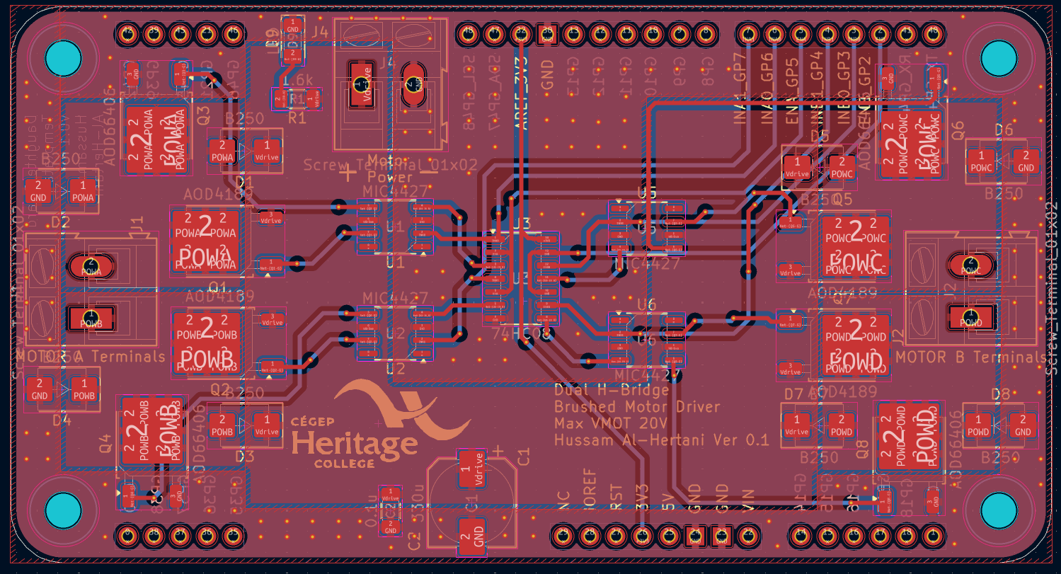
The layout of the H-bridge is shown in Figure 3. Instead of using wide traces to route the high current nets in the design, we chose to use zones in the top copper layer. If you look closely, you’ll notice
- POWA & POWB zones for H-bridge ‘A’ on the left-hand side
- POWC & POWD zones for H-bridge ‘B’ on the right-hand side
- Vdrive zone shaped like a ‘U’ in the center of the board
- GND zone around the board and in the center of the board
The bottom copper fill is all set to the ground net.
By using zones in this manner, we avoid having to route the high current traces and maximize the current-carrying ability of the nets in the high current paths. We also beefed up the thermal reliefs to improve current transfer into/out of the various components.
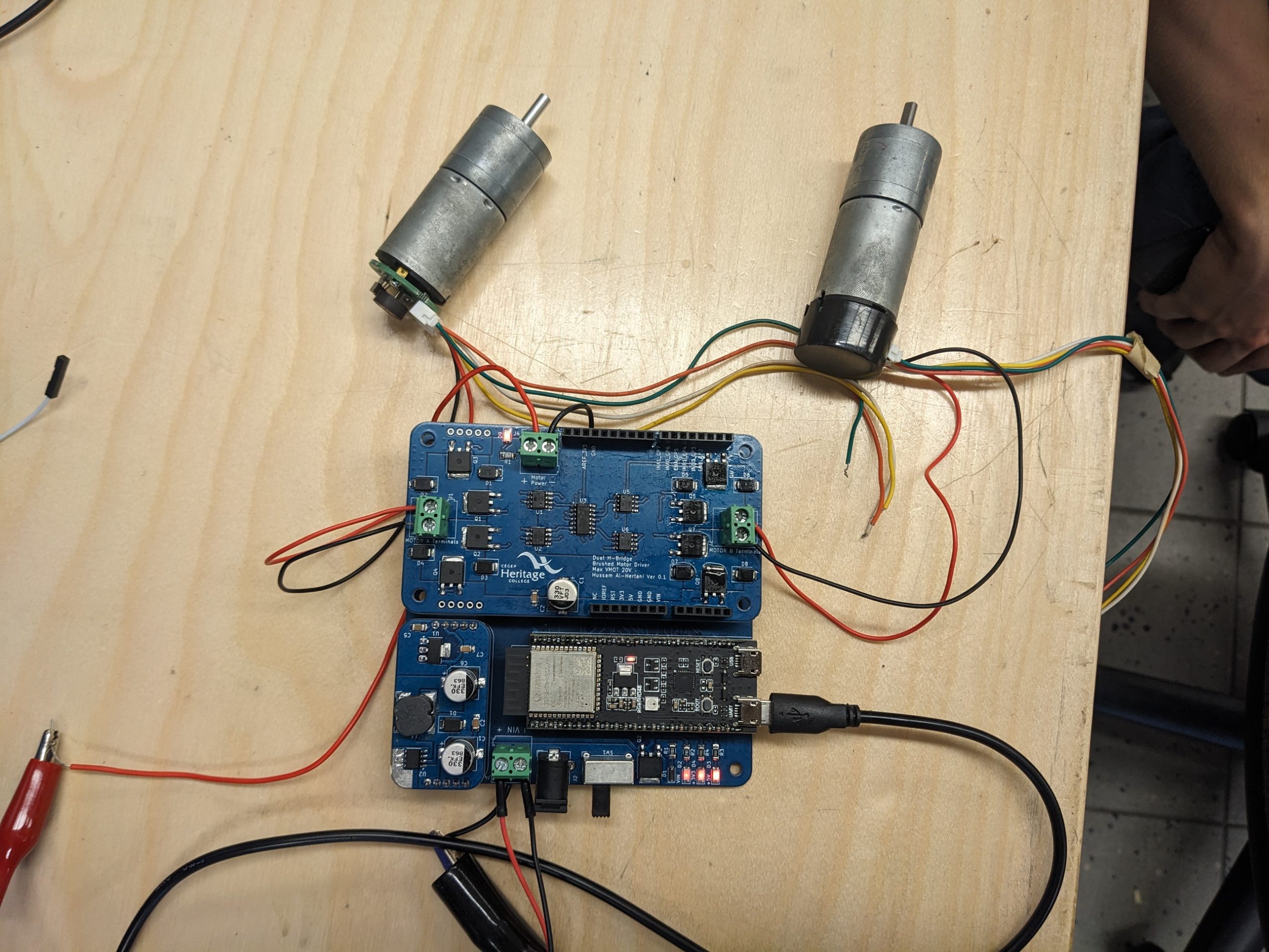
Design in action
The complete IoTIS platform with the dual H-bridge daughterboard is shown in Figure 5.
The complete KiCad files for the Dual H-bridge Daughterboard are available here. My KiCad library containing the daughterboard symbol and empty footprint outlines is also available.