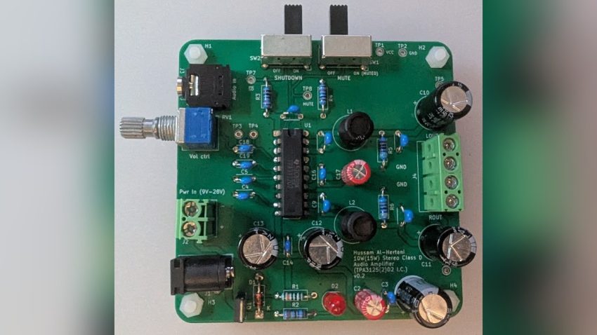
In this blog entry, the design of an all through hole class D amplifier board based around the TPA3122D2 (or the pin compatible TPA3125D2) IC will be covered.
The TPA3122D2 & the TPA3125D2 are the only through hole class D amplifier ICs that I’m aware of. The TPA3122D2 IC is a stereo 15W class D amplifier that comes in a 20-pin DIP package, and requires a relatively simple LC filter at it’s output.
While the TPA3122D2’s part status remains ‘Active’ on the TI site, notices have been circling around the internet that its part status will soon become ‘not recommended for new designs’. Fortunately the pin compatible & through hole TPA3125D2 IC’s part status is expected to remain ‘Active’ for a while. The TPA3125D2 is almost identical to the TPA3122D2 with the exception that it’s output is rated for 10W (stereo) as opposed to 15W. This means that this board design could still be used with the TPA3125D2 long after the TPA3122D2 IC becomes NRND/Obsolete.
The schematic design is shown below and closely follows the recommended schematic in the datasheet:
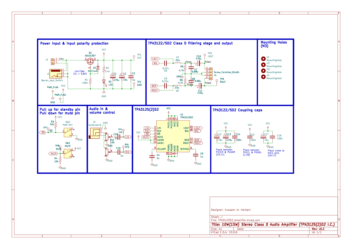
The circuit design is simple enough:
- Power (10-30V) is brought onto the board via either a terminal block or a DC barrel jack.
- A reverse polarity protection circuit protects the boards power rails.
- Audio signal to be amplified is brought onto the board via a 3.5mm audio jack.
- A dual gang potentiometer is to control the volume of both left and right channels at the same time.
- The LC filter design attached to the IC’s output is the one recommended in the datasheet
- A 4-pin terminal block is used to attach two passive speakers (left and right) to the amplifier & LC filter output.
- Plenty of bypass capacitors used to keep the power rails and output traces noise free.
- Two SPST switches used to shutdown the amplifier and mute it via control signals available on the IC.
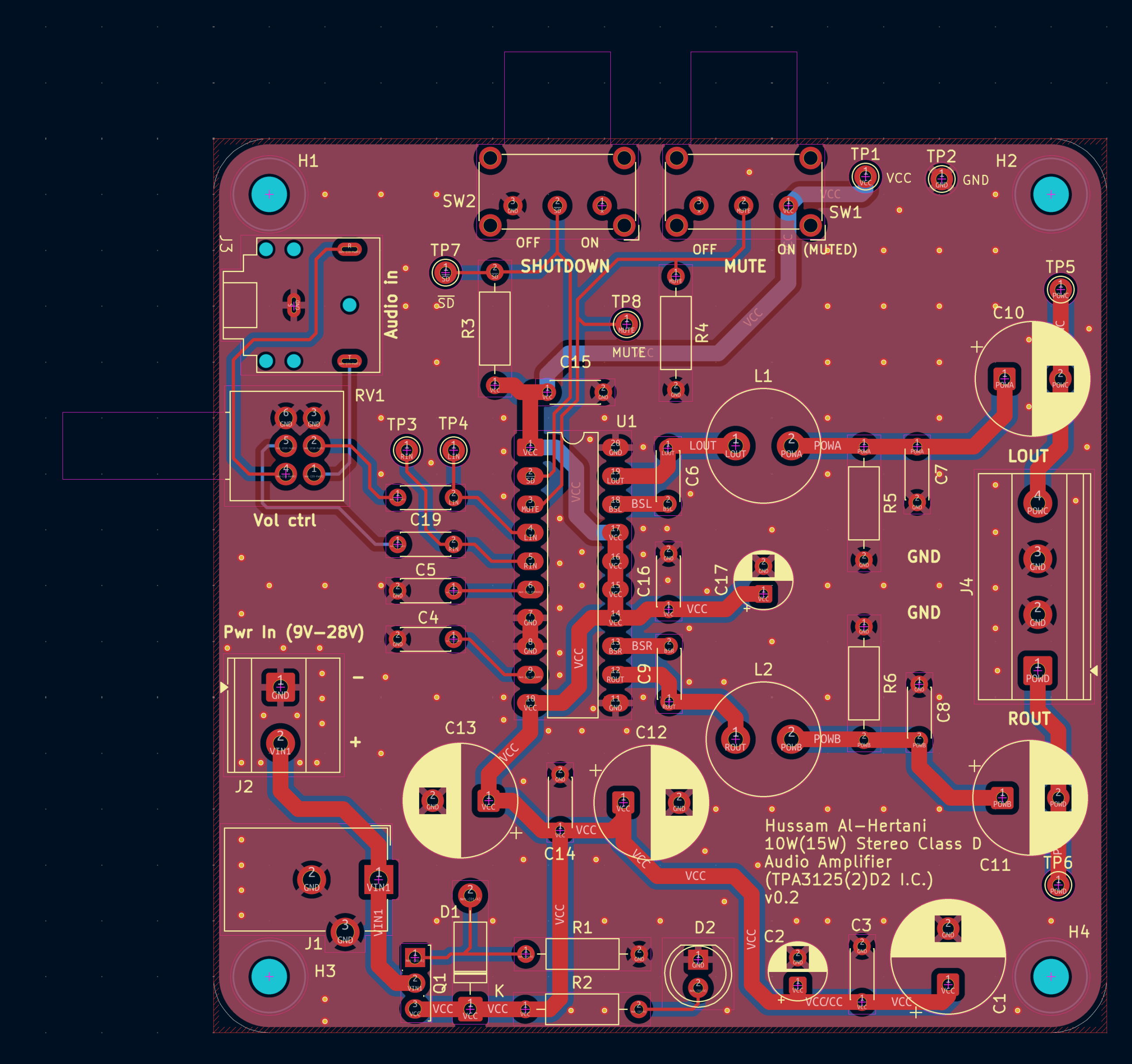
The PCB Layout is very a simple and clean 2-layer design. Board size is 80mm x 80mm.
The board was fabricated, populated and tested successfully. It amplifies audio well and produces decent audio quality and volume with a good set of passive speakers. An old laptop battery charger (19.5V) does a good job of powering the board.
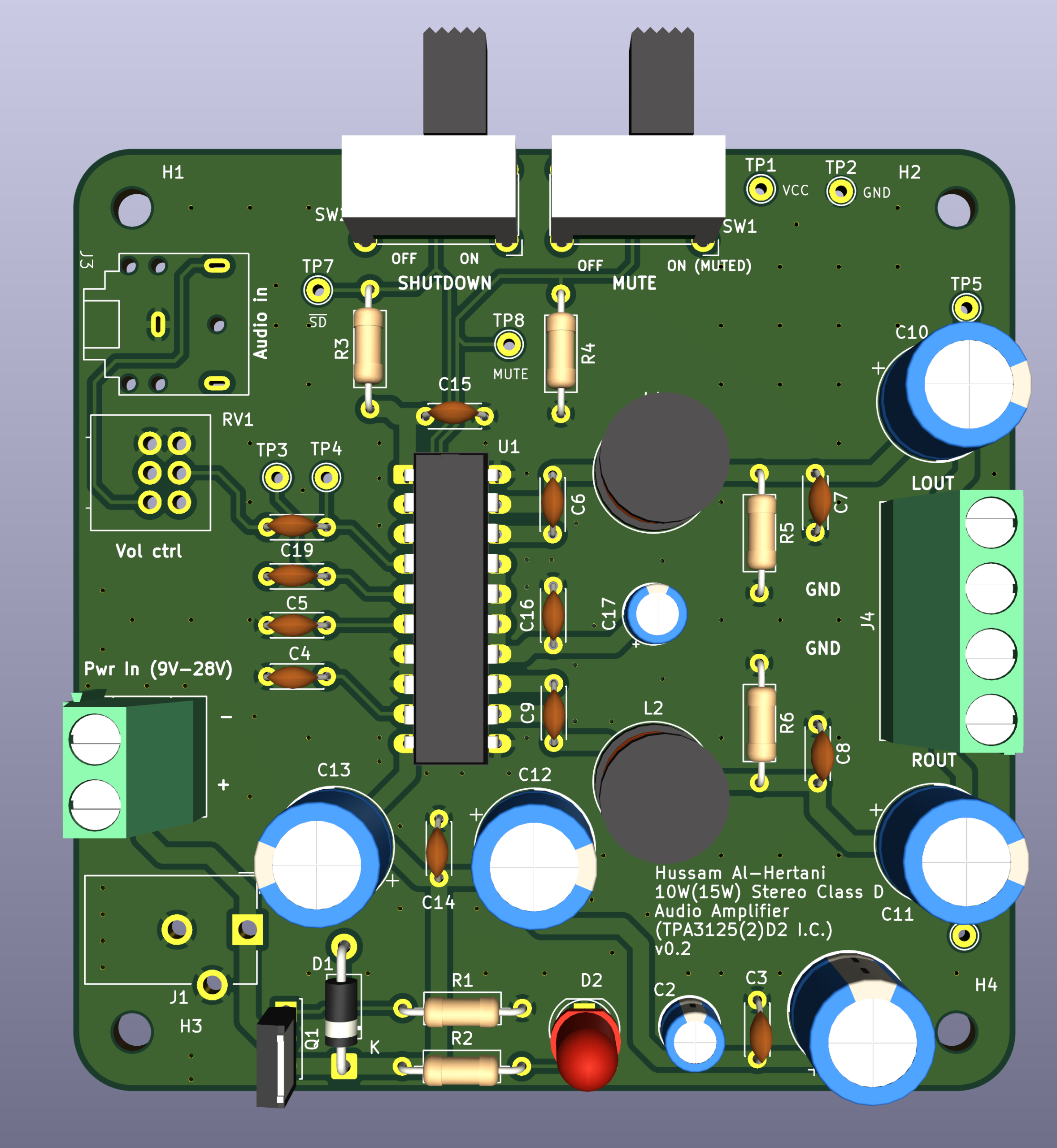
Overall this is a great design and makes for a great ‘introduction to soldering” kit. It is an excellent project for those trying to learn PCB layout design in KiCad. You can start with the provided schematic then create your own layout. KiCad Files for this project including Digikey BOM are available at this github repo.