The EET Faculty at our college decided to develop a standardized printed circuit board (PCB) platform that students can utilize in their capstone projects. It’s called the IoT Innovation Station (IoTIS), and is sometimes referred to as the ‘IoT stack’.
In addition to serving as a standardized platform for the program’s capstone project, students get to learn about PCB circuit design and KiCad by designing the layout and populating their own IoT stack ecosystem of boards in earlier project courses.
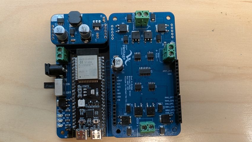
The IoTIS platform consists of the following four boards, shown in Figures 1-6:
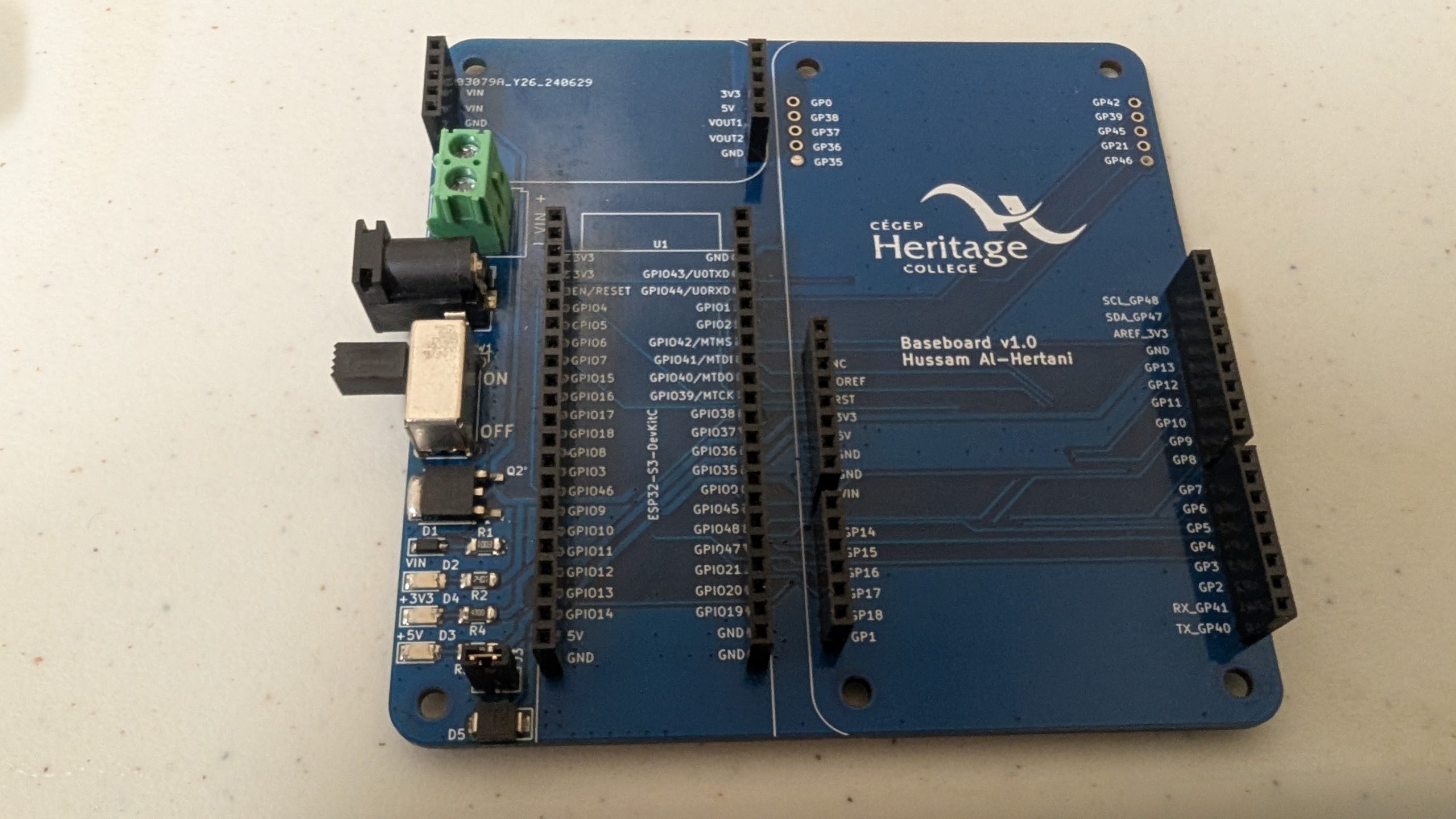
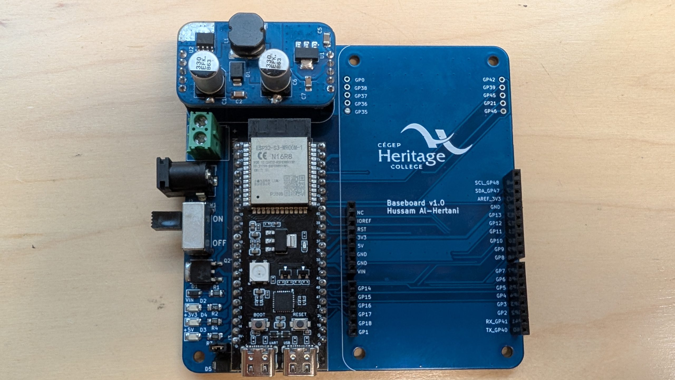
- The baseboard: This board accepts input power (12-7V) via either a DC barrel jack or a terminal block and provides power(VIN rail) to all the other boards. It also hosts headers that hold and connect the other IoTIS components / PCBs.
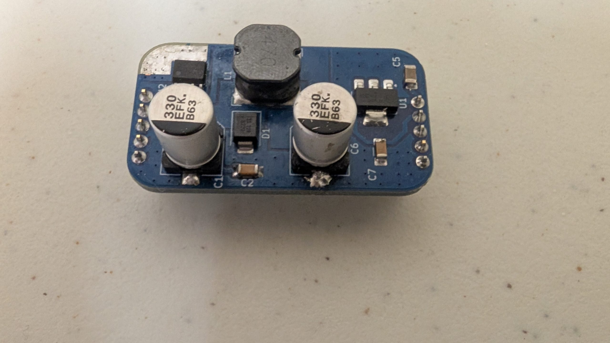
- The powerboard: This board plugs into the baseboard via headers and is responsible for generating the +5V and the +3V3 rails utilized by the daughterboard.
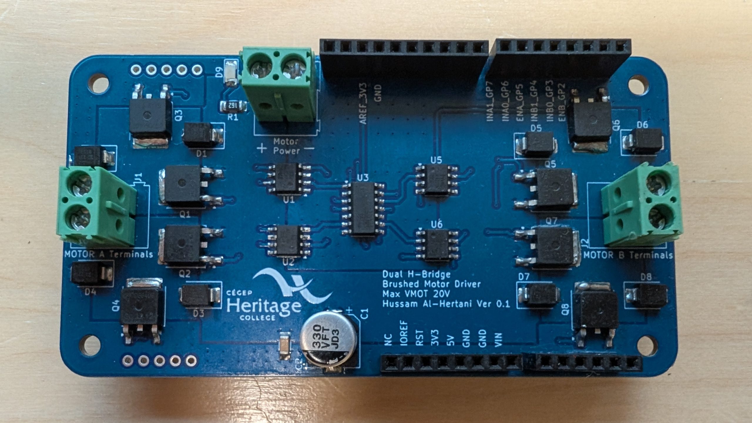
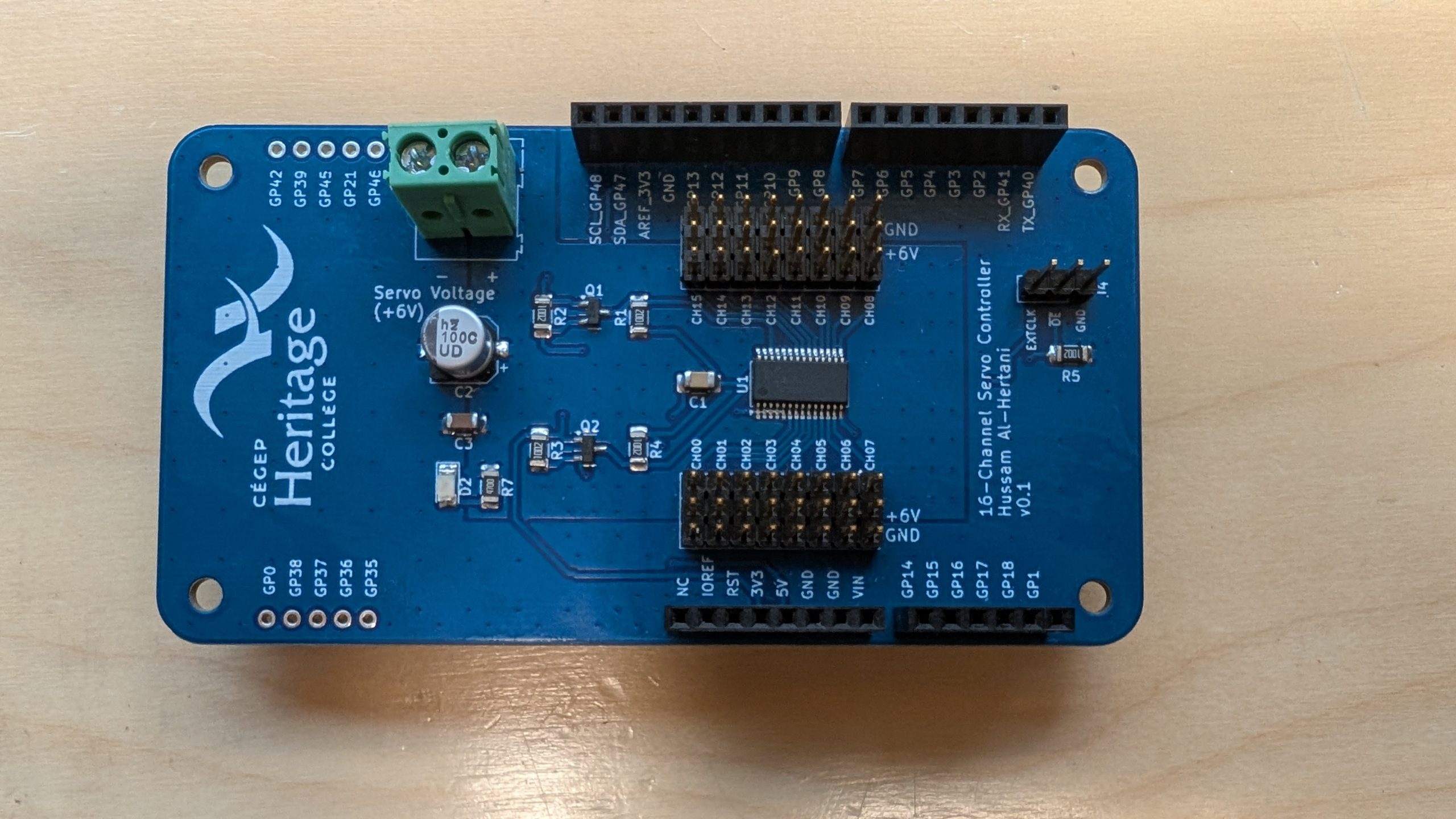
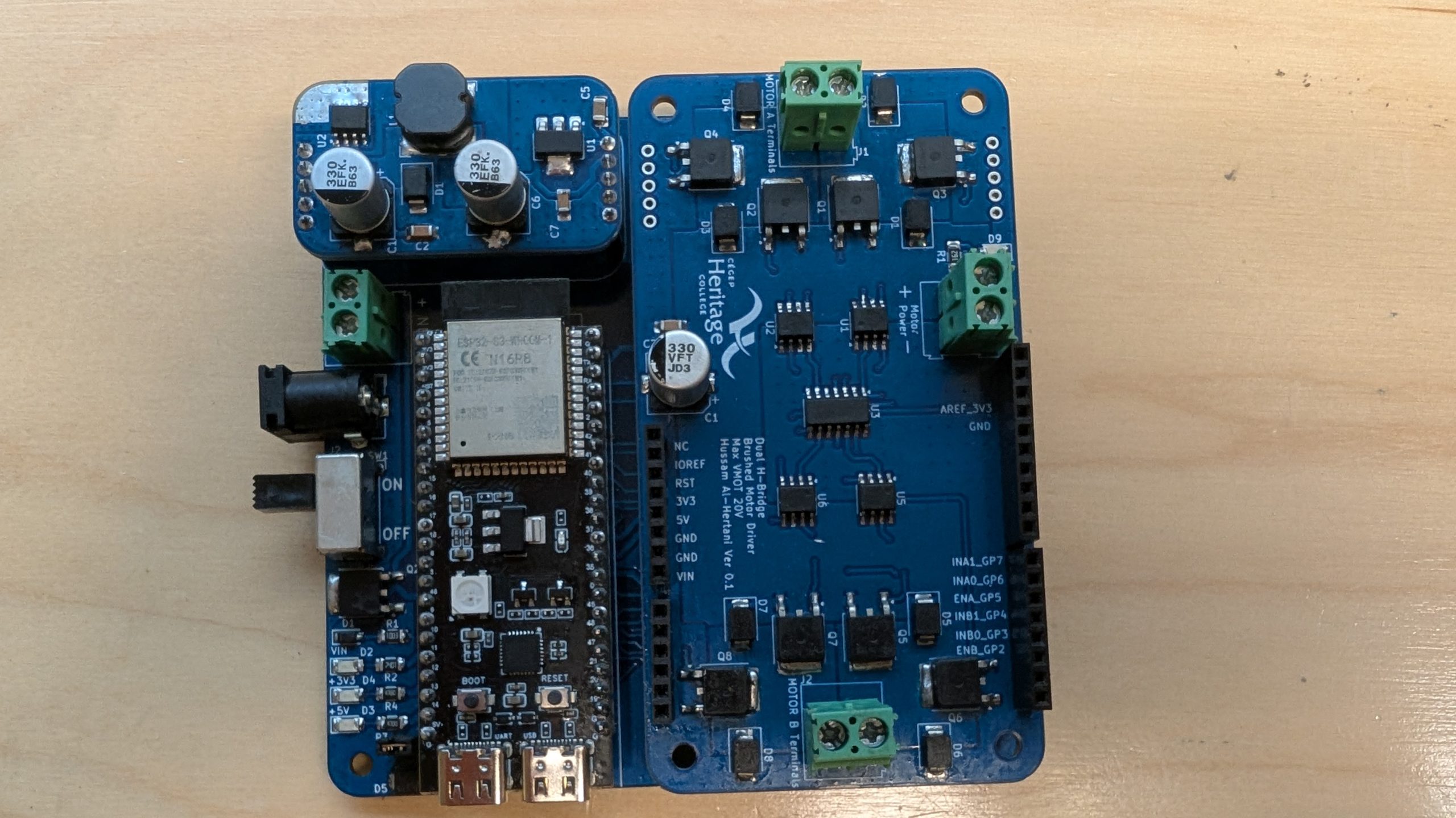
- The daughterboard: This board also plugs into the baseboard and includes the capstone-specific components and circuit design. The daughterboard is Arduino shield compatible. Figures 3 and 4 display two different daughterboards that were developed as reference boards: i) The dual discrete H-bridge motor controller daughterboard and the PCA9685-based 16-channel servo controller daughterboard.
Figures 5 and 6 show what the complete IoTIS platform looks like without a daughterboard (Figure 5) and with a daughterboard (Figure 6).
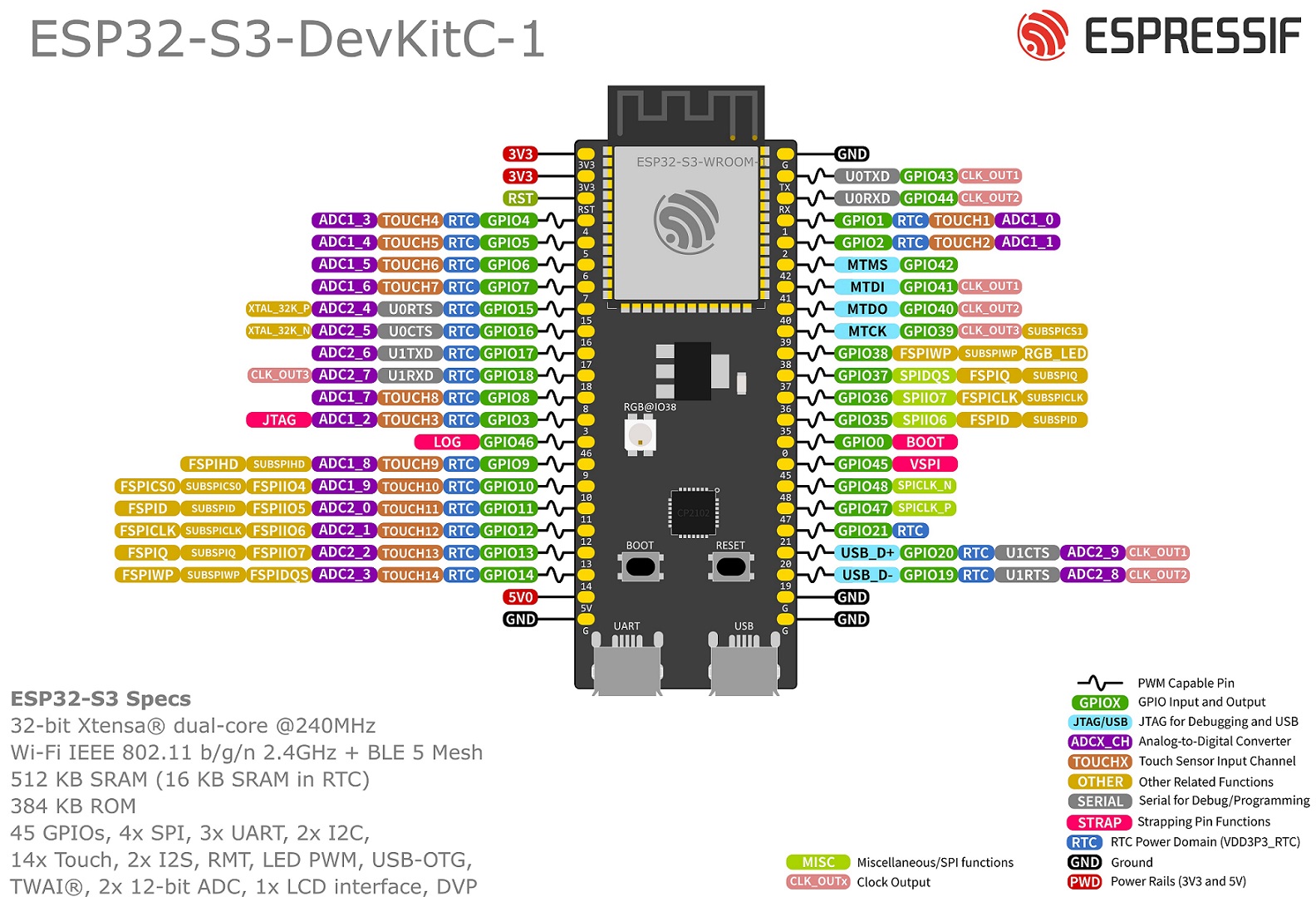
- The ESP32-S3-DevkitC-1 development board. This is the official ESP32S3 development board from Espressif. The pinout of the development board is shown in Figure 6 for reference.
IoTIS GPIO Pins
The IoTIS platform brings out all of the development board’s pins to the daughterboard, with the notable exception of the UART0 debug port (GPIO43/ GPIO44) pins and the USB (GPIO19, GPIO20) pins, as these are already attached to connectors on the development board.
Here’s a summary of the usability of ESP32-S3-WROOM pins:
- Cannot use: GPIO26-32 (Flash), power/ground pins, USB pins (19,20), GPIO43/44 (UART0)
- Limited use: GPIO0 (external 10kΩ pull-up ), GPIO3, GPIO45, GPIO46 (external 10kΩ pull-down) (strapping).
- JTAG pins: GPIO39-42 (can use if JTAG is not needed)
- PSRAM pins (if present): GPIO33-37 (cannot use on PSRAM variants)
Keep in mind that for the PSRAM variants of the ESP32-S3 devkitc-1 board, the truly “safe” GPIO pins are significantly reduced to: GPIO1, GPIO2, GPIO4-GPIO18, GPIO21, GPIO38, GPIO47, and GPIO48.
The daughterboard makes available pins GPIO1, GPIO2, GPIO3, GPIO4-18, GPIO47, GPIO48, GPIO40 & GPIO41 on the lower standard arduino shield pins. Of those, GPIO3, GPIO40, and GPIO41 (as well as pins GPIO39 & GPIO42 on the non-arduino shield connectors) are typically used for external JTAG debugging. Since USB JTAG can be used instead of external JTAG, external JTAG debugging mode is typically disabled, making these pins available for GPIO use. The only precaution is to ensure that GPIO3 is either floating or low while the microcontroller is booting, as the state of GPIO3 at boot enables external JTAG debugging mode when high, and disables it when floating or low.
The two non-Arduino shield 5-pin connectors at the top of the daughterboard bring out the remaining pins. Of those, you can really only use GPIO39, GPIO42, GPIO21, and GPIO38 if your microcontroller is a PSRAM variant (most of these development boards are). If not, you may also be able to utilize pins GPIO35-37.
Powerboard schematic and layout
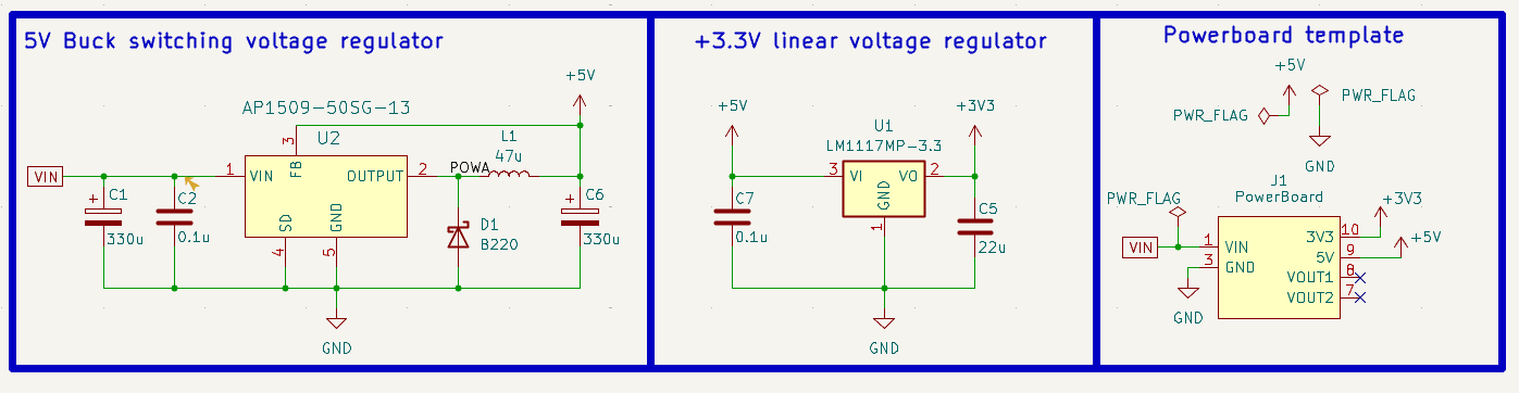
The powerboard consists of a 5V Buck regulator that generates a +5V rail from the VIN rail (coming from the baseboard), followed by a 3.3V linear regulator that produces a +3.3V (+3V3) rail from the +5V rail.
The Vin rail is typically 12-7V. The front-facing +5V Buck regulator can efficiently (power efficiency) drop this voltage to 5V while minimizing its own power dissipation, despite its 7V-2V dropout voltage between the input and the output.
Because the incoming 5V input is only 1.7V higher (1.7V dropout voltage) than the 3V3 regulator output, and because the 3V3 rail isn’t expected to draw much current, a linear 3V3 regulator was selected instead of another 3V3 Buck regulator. In this case, the power requirements for the 3V3 regulator were so low that the regulator’s power efficiency was not a priority, as in the front-facing 5V regulator. The linear regulator also requires fewer components (inductor and diode are not needed), provides a ‘cleaner’ (less noisy) output, and is simpler to use than a Buck regulator.
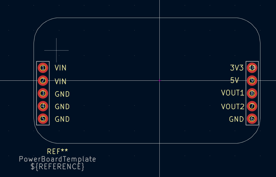
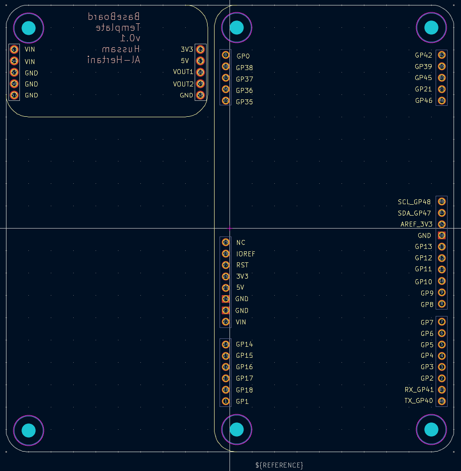
As shown in Figure 8, the powerboard was built as a template. i.e., a powerboard symbol was created and attached to the powerboard outline footprint shown in Figure 9. This footprint contains the powerboard’s board edge and pinout only. Allowing the designer to modify the circuit design shown above if necessary.
To create a new Powerboard design, the PCB designer first creates their personal voltage regulation design, then drags the powerboard symbol into the schematic and connects all the power rail nets to the appropriate pins on the symbol. When performing the layout, the correctly sized board edge and properly spaced connector pins will already be there, saving the designer time and minimizing chances of error.
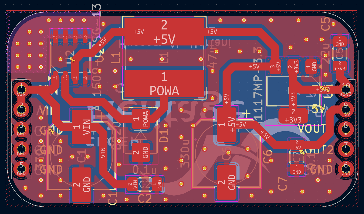
The powerboard PCB layout design is shown in Figure 10. The solder mask in the top right-hand corner of the board was removed. This exposes the top copper region connected to the ground pins of the 5V Buck regulator, allowing for better heat dissipation, further improving the regulator’s performance and efficiency.
Notice the two pins on the right connector labelled VOUT1 & VOUT2. These are left unused here, but could be used to generate additional voltage rails in custom designs.
Baseboard schematic and layout
The baseboard’s main function is to bring power into the IoTIS platform and hold the ESP32-S3-DevkitC-1 microcontroller development board, the powerboard, and the daughterboard. It then routes all the relevant ESP32-S3 GPIO pins and the power rail voltages (from the powerboard) to the daughterboard connector pins.
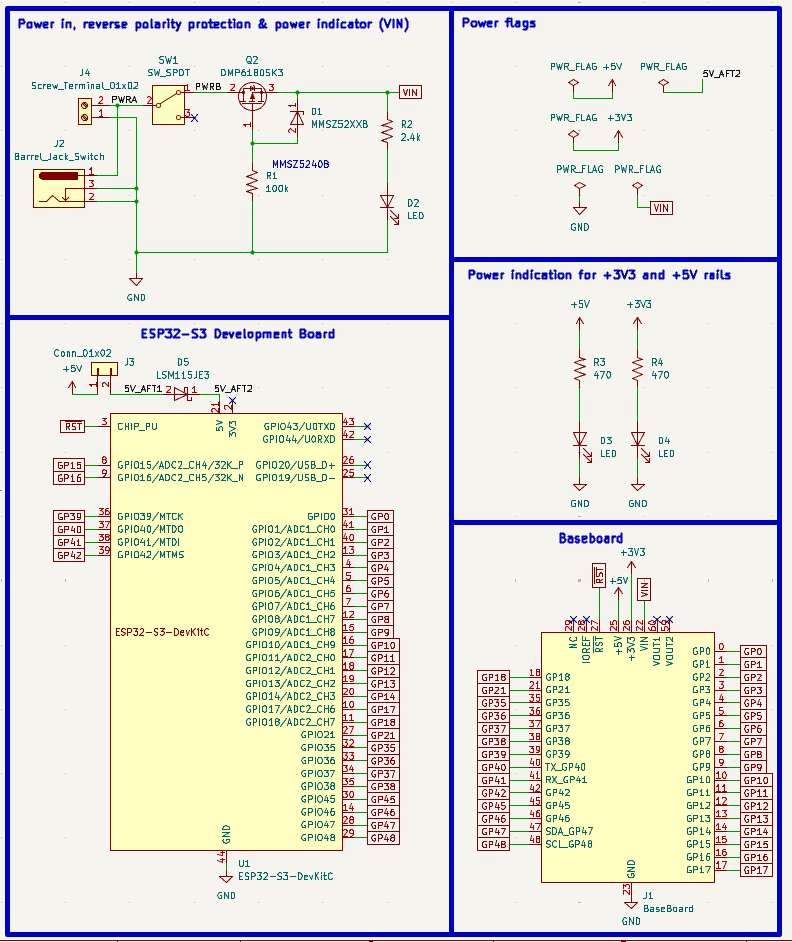
Power (7-12V) comes in via either a terminal block or a power jack. The power input circuitry includes a reverse polarity protection circuit (Q2, R1, and D1) and a Vin power LED indicator. The 3V3 and 5V rails coming from the powerboard are also routed to one LED power indicator each. This way, the user can directly monitor if any of the main rails are not functioning properly.
A Schottky diode was added in series with the input of the 5V pin on the ESP32-S3-DevkitC-1 microcontroller development board. This diode isolates the USB +5V from the +5V generated by the powerboard. Furthermore, it prevents the USB +5V from leaking from the DevkitC-1 board, into the baseboard & powerboard when the VIN rail is powered down. The jumper can be used to disconnect the DevkitC-1 board from the powerboard’s 5V rail if the programmer/user chooses to exclusively rely on USB power. This is sometimes required for testing. The jumper can also be used to measure the current consumption of the DevkitC-1 board.
As with the powerboard, the baseboard was also built as a template. i.e., a baseboard symbol was created and attached to the baseboard outline footprint shown in Figure 12. This footprint contains the baseboard’s board edge and pinout only. Allowing the designer to easily and quickly modify the circuit design shown above if necessary, while maintaining the same board shape, size, and pinout.
The completed layout for the baseboard is shown in Figure 13. It is messy! The ground plane below the DevkitC-1’s antenna was removed to improve signal reception. It turns out that this was not necessary as the DevkitC-1 board will be raised above the board with headers.
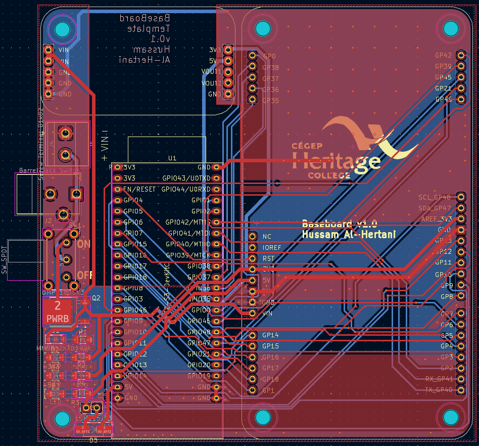
This particular layout doesn’t quite pass the design rule check. The diode D5 has a wider footprint than the space available and creates a courtyard overlap with the DevkitC-1 footprint & mounting hole. This error can be safely ignored since the DevkitC-1 will be raised above the baseboard via a pair of headers.
The Design files for the IoTIS can be found here:
- The baseboard
- The powerboard
- My KiCad parts library containing the powerboard and baseboard symbol/footprint templates
I will cover the design of two ‘reference design’ daughterboards in future entries.
1 thought on “The IoT Innovation Station”